The Semiconductor Industry, especially the frontend manufacturing segment, was one of the pioneers in using digital tools such as MES when it came to process execution. But, as it happens with most pioneers, complacency crept in and most manufacturers focused on updating their manufacturing capability and driving efficiency through improved production technology and increased Capex, rather than a simultaneous focus of upgrading and updating the very systems which could help them improve their operation exponentially. Thereby, in the present day and from an Industry 4.0 and digital transformation perspective, it is safe to say that the industry has a lot of catching up to do.
By Tom Bednarz
Most manufacturers use multiple point solutions coupled with legacy MES applications which are either extremely rigid to customize, and lack scalability, but owing to their mission-critical functional support, they are kept as a part of the process, which keeps getting more complex with increasing product mix, shorter lead times and elevated demand. When complex processes use multiple applications to execute individual tasks within a process, data capture and reporting gets undermined and with it the potential to gain better results from a performance and quality standpoint.
It is extremely important that leaders look at their existing process and recognize areas where gaps exist, and then plug those gaps using modern applications like a new and industry-specific MES platform. For example, a classic struggle for almost every semiconductor manufacturer is the dependence on manual execution methods or legacy customizations when it comes to handling a ‘send-ahead wafer’ scenario. Almost every manufacturing operation uses send-ahead wafers and yet, not many are equipped with an overarching application which has this capability as a native feature.
Send-Ahead Wafers, where does the problem lie?
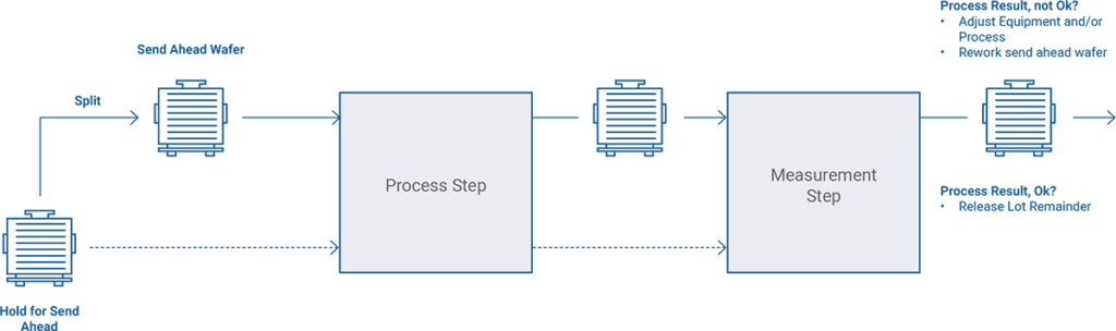
Taking the send-ahead wafers example further, all semiconductor manufacturers use this methodology to reduce scrap and adjust process parameters until they hit the right process configuration and spec conformity. The idea is simple: there is a (temporary) send-ahead lot usually containing one wafer and a ‘main/bulk lot’ with the rest of the wafers, waiting for the send-ahead results.
Depending on the send-ahead lot results, the next actions could be:
Accept the result and go ahead with processing the main/bulk lot using the exact same settings/parameters that were used for the send-ahead (thus confirming the settings);
Make some adjustments to the settings, based on the send-ahead results, and then go ahead with processing the bulk lot;
Depending on how big of an adjustment was necessary and how much the send-ahead lot results deviate from the target, the send-ahead lot may need to be reworked;
Depending on how easy it is to determine the necessary adjustments, another send-ahead may be required to confirm the adjustments deliver the expected results before going ahead with the bulk lot.
It is easy to understand with critical processes like etching, CMP and lithography, where the uncertainty of eventual output parameters dictates that send-ahead wafers be used to prevent larger scrap rates and generate better overall throughput. This has been the case for decades and will remain an important part of the overall process flow for decades to come. The goal for process owners to maintain proper cycle time and output is to ensure send ahead wafers are used to the minimum possible extent throughout the process, irrespective of the inherent complexity of a given product type.
Unfortunately, most legacy MES do not support this capability
This is where the problem lies, since most legacy MES applications do not support the send-ahead wafer capability. It is either executed manually, which makes tracking all parameters and maintaining the requisite throughput difficult; or worse, it requires extremely costly and time-consuming modifications to be made to the legacy application, which may still not meet the IoT enabled integration needs and may deliver only a sub-optimal performance with respect to send-ahead wafers.
eBook and Technical Guide - Advanced Capabilities in Semiconductor Manufacturing mockup1100x764px_2
Advanced MES Capabilities for Semiconductor Front-End Manufacturing
In totality, the impact of executing the send-ahead wafer facet of the process manually or with a modified legacy application can result in:
Increased manpower costs to perform operations, tracking and reporting manually of a semi-ready system. Availability of skilled personnel might also be a challenge, considering the otherwise automated nature of process execution in the industry.
When performed manually or using applications where data must travel through two or more applications, there is an inherent delay which impacts the overall cycle time; and if data entry is manual, this can lead to errors in in recording parametric data, which defeats the purpose of using send-ahead wafers.
Lack of traceability when performed manually is also a major challenge. When multiple process steps and recipe instances must execute in a complex operation, with several operations needing execution in an extremely specific order on a specific tool and chamber when executing send-ahead wafers manually, the ability of being able to precisely track, record, report and use the data to make improvements becomes a major challenge.
In a manufacturing environment where production runs are time-sensitive and the pressure from customers is high, the reduction of cycle times is a necessity. The thought of continuing to execute send-ahead wafers manually or through a customized legacy tool directly translates to increased cycle times, which then imply decreased throughput, efficiency and eventually business.
Send-Ahead Wafers should exist as a core application capability in your MES
When a send-ahead wafer is executed through the same MES which is also responsible for the overall process execution, all the delays and lack of traceability disappear. It’s because the same application which connects with and controls process scheduling, execution and equipment now also schedules, orchestrates and executes send-ahead wafer lots.
The ability to split a production lot such that the send-ahead lot or wafers are processed in the least possible amount of time, with complete traceability, parametric recording and automated process or equipment adjustment before the bulk lot is processed or a second send-ahead wafer lot is issued, can all be controlled and executed through the same MES platform. For process owners, this is the fastest way to ensure critical process steps are executed with minimum wastage of time, capacity, labor and material, with highest possible visibility and throughput.
When performed through the MES, the challenges pertaining to using excess manpower and the cost therein are eliminated, as the system executes the operation automatically and as a part of the overall orchestration plan. Since all metrology and parametric records are obtained either directly from the equipment via IoT or through integration with the automation application, the receipt, reporting and analysis of data is near real-time, with no possibility of errors and complete elimination of time lag. Further, since the same application which executes bulk lots also executes the send-ahead wafers and performs the split and merge operations as needed, there is complete traceability. Finally, with a single platform, there is no case for additional integration, manual recording or expensive and extensive customizations, which makes performing the send-ahead wafer tasks wallet friendly as well.
Leaders and managers of semiconductor fabs need to look beyond their existing legacy tools and avoid the ‘this is how we have always done it’ mind set, to see the transformative benefits gained when this advanced capability exists as a part of the MES core functionality. With native advanced capabilities, the right MES can leapfrog the existing operation from a reactive to a proactive operation and help improve data capture and analysis accuracy, enhance cycle times and help meet Industry 4.0 deliverables through edge computing and automation.
Source https://www.criticalmanufacturing.com/blog/send-ahead-wafers-why-this-advanced-capability-should-be-native-in-your-mes/


