This article is an opinion of Jaswinder Ahuja, the Corporate Vice President and India Managing Director for Cadence Design Systems Inc.
The importance of the semiconductor market has reached new heights due to the rising demand for sophistication, automation, and intelligence in various electronic systems. This has resulted in a surge in the number of chips being used in different domains, leading to the need for specialized and complex semiconductor chips. Industries across various fields are embracing digital transformation, further fueling the demand for advanced semiconductors. The significance of semiconductor chips has become even more apparent with the emergence of technology trends such as AI, industry 4.0, autonomous vehicles, 5G, and edge computing. The exceptional demand for these cutting-edge semiconductors is driving the growth of the semiconductor market, and McKinsey & Company has predicted that the industry will reach one trillion by the end of the decade.
The rapid development of emerging technologies has created a need for high-performance, low-latency, and pixel-heavy computing that requires larger and more complex electronic components. The cost of advanced processes is becoming increasingly high, and with Moore's law slowing down, the industry is focusing on achieving the right balance of integration, functionality, and density at the right price.
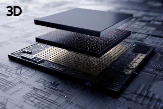
To reconcile the technology needs with increased expenses, the semiconductor industry is moving towards heterogeneous integration, or 3D-IC. This involves designing smaller, specialized or optimized chiplets and stacking them in a disaggregated SoC architecture to reduce costs, mitigate risks, and speed up time-to-market. 3D-IC also allows for greater flexibility and supports the spirit of Moore's law by reducing package size while maximizing functionality.
Advanced packaging has become a critical aspect of the industry, adding value and differentiation. 3D-IC is a significant promise, with the global market expected to reach $51.81 billion by 2030. However, the transition to a new ecosystem requires time and effort, and the 3D-IC floor must be ready.
India has a massive consumer market for electronic products and a significant pool of skilled workers, making it an excellent opportunity to create a local semiconductor ecosystem. The government's new policies and schemes, such as Make in India and Production Linked Incentive (PLI) and Design Linked Incentive (DLI), are accelerating India's dream of becoming a global hub for electronic system design and manufacturing. The 3D-IC chiplet space also has significant possibilities to grow and create a market space for commercial third-party chiplets, allowing India to build expertise and become a key player in the semiconductor industry.
The semiconductor industry is moving towards heterogeneous integration, and India has an opportunity to capitalize on the high demand for semiconductors by developing a local ecosystem. By investing in the 3D-IC space, India can build leadership, gain expertise, and become a key player in the semiconductor industry. This requires collaboration and the creation of an empowered group of technocrats under the India Semiconductor Mission to define the strategy and march towards the future of advanced packaging built in India.


