Why is Intel struggling to reach 7nm (2023 now) while being much bigger and richer company than AMD who is already on 7nm? 7nm is already available from many companies but not from Intel.
First of all: AMD does not manufacture its chips. AMDs current-generation chips are manufactured by TSMC.
And second: “7nm” is ONLY a marketing term.
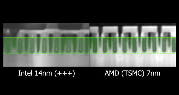
The so-called “10nm” Intel is now using in the latest mobile chips is actually slightly smaller than TSMC’s manufacturing process called “7nm”; The most important measurement of a chip is the pitch of two metal wires. This is 40nm for the TSMC “7nm” (N7) process but 36nm for intels “10nm” process.
Something like 15 years ago, the “nanometer number” was a real physical measurement inside the chip. But then it became hard to decide what to measure, so the companies just started calling their new processes with a number than was about 0.7x times the “size number” of their previous process. This was ok for the next 10 years, when the next process really was twice as dense as the previous one, like 0.7x shrink should give.
But then TSMC, Samsung and Globalfoundries made their “20nm” processes which simply sucked in performance because of leakage problems. Almost nobody wanted to use them, and the GF 20nm process was cancelled. In order to get the leakage down, they had to switch to finfet style transistors (Intel had already switched to finfets in their “22nm” process).
When TSMC introduced finfet transistors, it did not shrink the process at all. It still had the same size than their “20nm” process, but it performed like the “20nm” process SHOULD have performed. When Samsung and GF introduced their (commonly-developed) finfet process, it only shrank some measurement very slightly, it was almost as big as their “20nm” process.
But because these “fixed 20nm finfet processes” were much better (in performance, not density) than the sucky original “20nm” processes they were replacing, for marketing reasons they decided to call them “16nm” (TSMC) and “14nm” (GF and Samsung).
And then when they made their next process, which might have “deserved” the name of “14nm” or “16nm” based on their density, they gave it name “10nm”. And the next one got name “7nm” (N7). But also, in these process changes, the density did not increase by a factor of 2x like it should have been, 7nm process should be 5.3 times more dense than 16nm process (16/7)^2 = 5.3, but in reality the TSMC N7 process is only 3.1x more dense than TSMC’s “16nm”, which should only deserve name “20nm” based on density.
So, the process Intel was originally going to call “7nm” process will be smaller than TSMC’s “5nm” process (N5).
Edit: But Intel just renamed their processes in 2021. They started calling improved version of their “10nm” prosess “Intel 7” to have more similar numbering than TSMC and Samsung. Though then Samsung also started calling improved version of it’s “7nm” process “5nm” even though it’s density is very close to the density of Intels “10nm”, “Intel 7” and TSMC’s “7nm” (N7) process.
So, in reality the situation is that currently we have TSMC mass-producing reliably huge amount of chips with 40nm metal pitch, using 193nm DUV equipment with multi-patterning, while Intel is manufacturing smaller amount of chips with 36nm metal pitch with similar 193nm DUV equipment with more agressive multi-patterning, and not getting as high clock rates from them as it wants.
And because Intel is not getting high enough clock speeds from this process, Intel also keeps manufacturing desktop chips with their older “14nm” process which has 52nm metal pitch.
TSMC has already started low-volume manufacturing of new processes (“N7+” , “N6” and “N5”) which use 13.5nm EUV equipment and does not need such aggressive multi-patterning. The “N7+” is probably going to be quite similar to Intel’s “10nm” in density, but the new EUV equipment means aggressive multi-patterning is not needed.
The TSMC’s “5nm” (N5) is a denser process, but Intel’s “7nm/Intel 4” process will be denser than TSMC’s “5nm” (N5).
The main reasons why Intel’s “10nm” process was late were probably:
They tried to improve too much at once. TSMC and Samsung no longer try to make their new processes 2x denser and simply just cheat on their marketing nanometer numbers, while Intel tried to make a process that’s about 2.2x denser than their previous “14nm” process. It’s much easier to make small changes than big changes.
They try to make very small features with big 193nm wavelength equipment with very aggressive multi-patterning. TSMC is not having as small features in its “7nm” (N7) process, Samsung is not having as small features in its “8nm” process and both are moving to 13.5nm EUV quipment to manufacture so small features (Samsung in their “7nm” process, TSMC in their “N7+”, “N6” and “N5” processes). Intel is only moving to 13.5 EUV equipment with their “7nm” process which will then be smaller than TSMCs “5nm” (N5) process.
They introduced some interconnects made from cobalt. New materials are always risky.
And Intel’s “7nm” (edit: now to be called “Intel 4”) is mostly late because they had to get their “10nm” working first. Many of the engineers that were supposed to be developing the “7nm” (now “Intel 4”) process may have been working on fixing the “10nm” (now “Intel 7″)instead. And there were probably some things in the “7nm/Intel 4” process which were supposed to be based on the “10nm/Intel 7” process, when the “10nm” process had not stabilized they could not just take them from there.
So, when Intel’s “7nm/Intel 4” process will finally come, maybe in 2023, it will be denser than TSMC’s “5nm” N5 process, but TSMC might already have their “3nm” process (N3) out by then. TSMC’s “3nm” (N3) process might be slightly, but not much denser than Intel’s “7nm” (N4).
Special thanks to Mr. Heikki Kultala, Technical lead, SoC architecture at Nokia.


