Rosatom and the Russian Academy of Sciences will develop a powerful EUV photolithography machine for the production of microelectronics. Academician of the Russian Academy of Sciences Alexander Sergeev, scientific director of the National Center for Physics and Mathematics (NTsFM, Sarov, Nizhny Novgorod Region), spoke about this in an interview with Expert magazine, published on Monday.
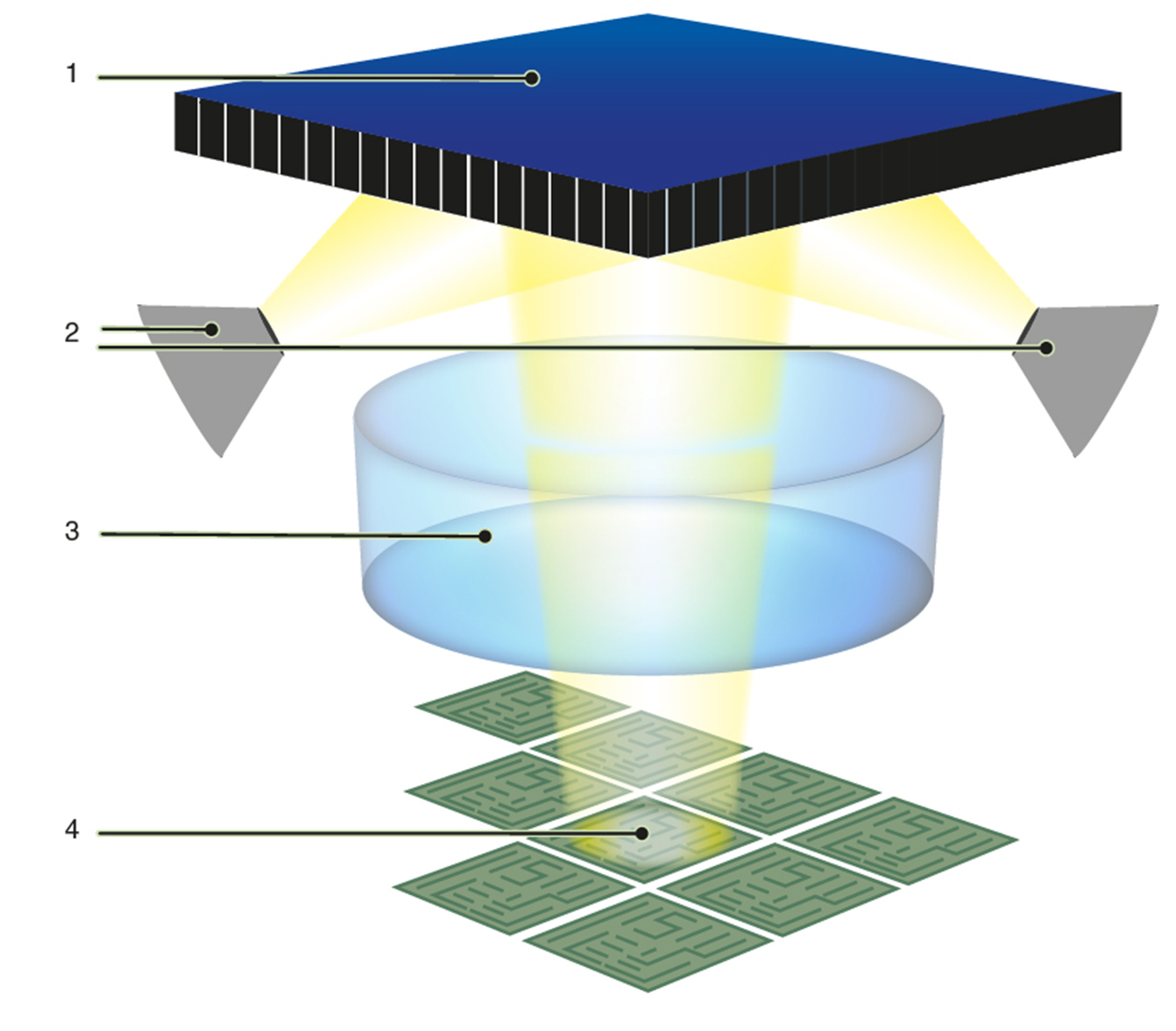
"This is a project in which several of the largest institutions of Rosatom and academic institutions plan to participate. I'm talking about a lithography machine based on laser-plasma interaction, when you have a powerful laser and a laser target in the form of a drop of substance or a jet of gas, which, turning into plasma, become the sources of X-ray emissionb. Highly reflective X-ray mirrors are very important here, because they allow this radiation to be concentrated, transported and used to draw various nanostructures on the photoresist," Sergeev said. According to him, Russia has all the necessary components for this, which must be combined in this development. "Firstly, a powerful laser. Rosatom has multikilowatt lasers that are used in various applications. Secondly, the technology for manufacturing X-ray mirrors, for example, at the Institute of Physics of Microstructures of the Russian Academy of Sciences, we have one of the best in the world. We can also use the developments of Rosatom to model this entire system based on a digital twin," the scientist listed.
Sergeev recalled that the world's first successful development of an X-ray lithograph was carried out by several national laboratories of the US Department of Energy, an analogue of Rosatom. According to him, the Russian institutes also participated in this program. “Today we need a similar cooperation of strong institutions, and it seems to me that it is in x-ray lithography that we can provide the country with an installation. Taking into account our scientific background, in general, we get a project that we need to urgently take on and do it,” summed up academician Sergeev.
Photolithography is a method of obtaining a certain pattern on the surface of a material, which is widely used in microelectronics and other types of microtechnologies, as well as in the production of printed circuit boards. One of the main techniques of planar technology used in the manufactureing of semiconductor devices.


