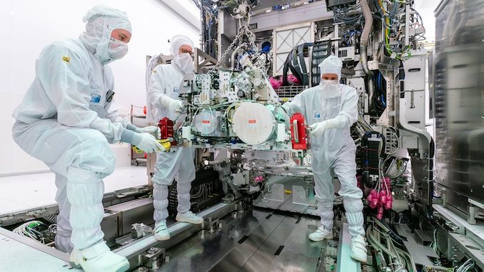
ASML is set to deliver the industry's first High-NA extreme ultraviolet (EUV) lithography scanner by the end of this year, marking a significant development in the next generation of EUV lithography machines. The machine in question is the Twinscan EXE:5000 pilot scanner with a 0.55 numerical aperture (NA). It is designed to enable chipmakers to learn and optimize the efficient use of High-NA EUV technology. ASML plans to commence high volume chip manufacturing using High-NA scanners in 2025, coinciding with the shipment of the commercial-grade Twinscan EXE:5200 scanner.
ASML CEO Peter Wennink acknowledged that there were minor delays in the assembly process due to difficulties faced by some in ramping up production and meeting the required technological quality. Nonetheless, he reconfirmed that the first shipment is still scheduled for this year.
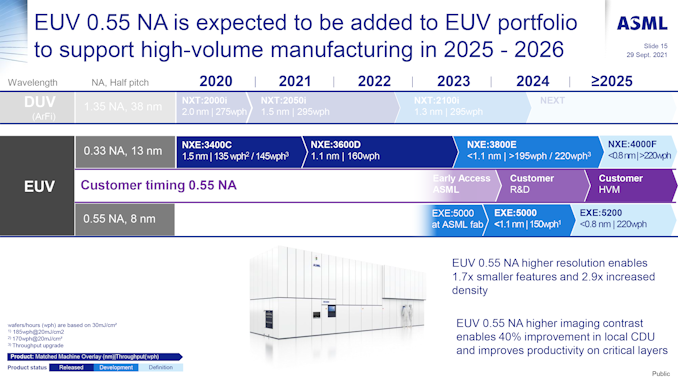
Currently, ASML's most advanced EUV scanners in various fabs are the Twinscan NXE:3400C and NXE:3400D, equipped with 0.33 NA optics, delivering a resolution of 13 nm. This resolution is suitable for manufacturing with metal pitches ranging from 30 nm to 38 nm. However, as chip pitches continue to decrease beyond 5 nm, a resolution of 13 nm becomes inadequate, necessitating the use of EUV double patterning and/or pattern shaping technologies. To address this, the industry is focusing on the development of High-NA EUV scanners with a 0.55 NA, aiming to achieve an 8 nm resolution for manufacturing technologies in the latter half of the decade.
ASML's High-NA scanners will require new optics and a larger light source, leading to significant investments and necessitating new fab structures. While the High-NA scanners themselves are expected to be significant investments, estimated at $300-$400 million per unit compared to over $200 million per 0.33 NA EUV scanner, they are crucial in enabling advanced manufacturing technologies.
Initially, Intel planned to use ASML's High-NA tools for its 18A (1.8 nm) production node, scheduled for high-volume manufacturing in 2025, coinciding with the anticipated delivery of the Twinscan EXE:5200. However, Intel later adjusted its plans and brought forward the commencement of its 18A production to the latter half of 2024. As a result, Intel is now expected to utilize ASML's Twinscan NXE:3600D/3800E scanners with two exposures, along with Applied Material's Endura Sculpta pattern-shaping system, to reduce the need for EUV double patterning.
Intel is anticipated to be the first customer to receive ASML's pilot High-NA scanner, allowing its developers and engineers to tailor Intel's process technologies to the upcoming production tools. The integration of these tools into Intel's processes is yet to be determined, given the timing of the tools in relation to Intel's own process node plans. Despite the uncertainties, since 18A is expected to be a long-term node, it is possible that Intel still intends to utilize High-NA EUV, even if it may not be viable initially.
Samsung Foundry and TSMC are also expected to commence chip production on their 2 nm-class nodes (SF2, N2) by late 2025. However, the role of High-NA machines in their plans remains uncertain at this time.


