The Japanese Canon Inc is developing a new generation of lithographic equipment for the production of semiconductors, capable of competing with the products of the Dutch ASML, which is practically a monopolist in the market for such solutions. The company will produce chip-making machines with advanced lithography, but without EUV. The construction of a new plant in Japan will also be a response to competitors' investments in the related field in the US, South Korea and Taiwan.
The investment is expected to be $345 million, including the cost of construction and installation of production equipment. The plant will start production in the spring of 2025. As a result, the company will double its production capacity in this niche. The company not only intends to expand production, but also relies on new technologies, thanks to which it will be possible to produce next-generation semiconductors at low prices. Today, it produces lithographic equipment at two factories in Japan, which is used to produce chips, for example, for car control systems.
The new 70000m2 plant will be built on the site of an existing production facility. This will be Canon's first new lithography facility built in 21 years, and construction will begin in 2023. In 2022, sales of lithographic equipment are expected to grow by 29% year-on-year to 180 machines - four times more than a decade ago. The new plant will meet the growing demand.
According to the World Semiconductor Trade Statistics, last year the global semiconductor market exceeded $500 billion for the first time in history. The industry expects it to exceed $1 trillion in 2030. Today, Canon controls 30% of the global lithographic equipment market by volume, second only to ASML, which accounts for 60%. Intel and Taiwan Semiconductor Manufacturing Co. (TSMC) have announced plans to build new in-house factories in the US and other countries. Canon decided to follow their example.
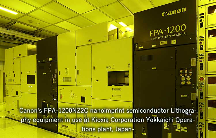
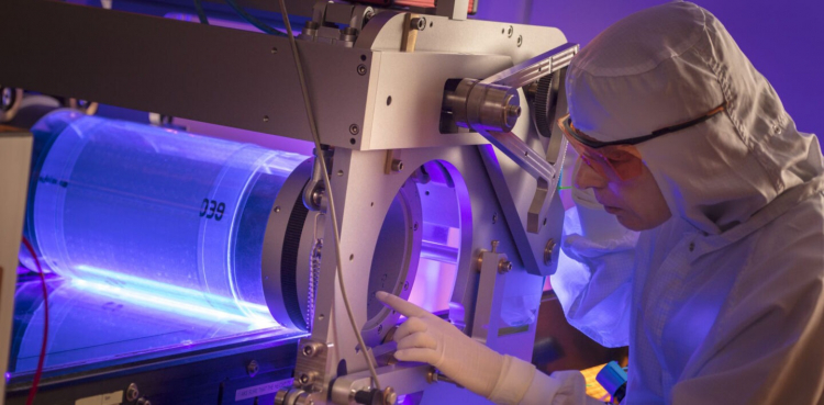
The company has also developed a next-generation technology called nanoprinted lithography. This makes it possible to produce the most advanced microcircuits at lower prices than existing lithographic equipment. The process is simplified thanks to a technique that allows you to literally "stamp" the drawings of integrated circuits, which can significantly reduce the cost of production - Japanese Kioxia and Dai Nippon Printing took part in the development of the technology.
Today, the technology that uses EUV lithography to form circuits at the nanometer level is the most indispensable technology. The only source of such technologies today is the Dutch ASML. However, such equipment is expensive, costing about $138 million per machine, and consumes a lot of energy. If nanoprinted lithography reaches the stage of practical commercial use, Canon expects to reduce the cost of lithography by up to 40% and energy consumption by up to 90% compared to EUV. This will shake the dominance of ASML in the market.


