Chinese scientists have made a significant breakthrough in producing a new two-dimensional (2D) material that is as thin as a single atom. This advancement is expected to facilitate the transition to next-generation semiconductors. The scientists have successfully used this new material to create 12-inch wafers, which could potentially complement traditional silicon chips.
The extremely thin nature of the 2D material gives the wafers excellent semiconducting properties. However, the scientists encountered challenges in scaling up the size of the wafers and achieving high-capacity production. In an exclusive interview with the Post, Professor Liu Kaihui of Peking University, the lead scientist on the project, expressed confidence in the practical applications of the 2D material. He stated that a transistor built from a single layer of the material outperforms a silicon-based transistor with the same thickness by a significant margin.
Each layer of the 2D material exists independently, enabling stacking layer by layer, similar to graphene or other transition metal dichalcogenides (TMDs) like molybdenum disulfide, tungsten disulfide, molybdenum diselenide, and tungsten diselenide. The team developed a new approach by using a surface-to-surface supply method, ensuring uniform growth.
According to Xue Guodong, a PhD candidate and the first author of the research paper, the fabrication of the MoS2 wafers involves using a chalcogenide crystal plate (ZnS) in combination with solution-dispersed molten salts (Na2MoO4) as an element source. This innovative method overcomes the limitations on wafer size.
Liu explained that the adopted strategy ensures even and sufficient supply of feedstocks in the furnace, solving the previous limitation in wafer size. Although larger wafers could be produced, the most commonly used size is the 12-inch wafers.
Once the size issue was resolved, the team focused on developing a strategy for batch production. Their proposed growth system is modularized and packed into a pillar-like structure, resembling the construction of a skyscraper. The gaps between the layers are filled with demand sources, resulting in highly uniform wafer growth.
This stacking method enables the simultaneous growth of multiple layers of 2D materials, leading to exceptional efficiency and low production costs. Liu proudly mentioned that their engineering team at the Songshan Lake Materials Laboratory has designed equipment based on this method. As a result, their equipment can produce 10,000 2D wafers per machine per year.
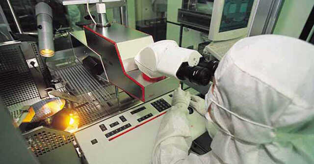
While successful fabrication of the wafers has been achieved, further steps are required to transform them into usable chips. These steps involve intricate design and engraving processes such as photolithography and deposition. However, Liu remains optimistic about the future of this technology.


