Onto Innovation has been slightly outgrowing KLA in inspection and metrology tools through standalone Optical Critical Dimension (OCD) tools in front-end fabrication as well as in the backend advanced packaging tools. SemiAnalysis believes these share gains versus KLA will accelerate. This is because our sources indicate that Onto Innovation has been selected by TSMC, Samsung, and Intel for critical metrology and inspection within next-generation processes utilizing gate-all-around nanosheet transistor architectures.
Generally, metrology and inspection equipment companies hold their own in a specific vertical within the space. Despite being a highly developed market with multiple competent players, there aren’t many market share shifts. A good example is Nova Measuring Instruments ($NVMI), which generally stays in its lane. They have a high share in integrated optical critical dimension (OCD) inspection tools and materials metrology tools. Meanwhile, they have little success outside these sub-segments.
The subsegments we wish to investigate today revolve around standalone OCD and thin film metrology and inspection. KLA has generally owned the thin film metrology and inspection market, with over 90% share of this market for certain tool types. Standalone optical critical dimension has generally been more competitive, but KLA also dominates this segment. This is especially true in FinFET transistor architecture and BEOL. This is mainly off the backs of their software suite and collector engineering.
Onto is looking to change this with their Atlas V product line. They are beating KLA at their own game by providing a superior metrology and inspection tool through better software and modeling with their “Ai Diffract” and “SpectraProbe” software suites.
While FinFETs utilize multiple P and N-type fins placed next to each other to form transistors. In the nanosheet architecture, multiple P or N-type nanosheets are built vertically. This provides more contact area per silicon area, improving performance and enabling higher density.

Intel, TSMC, and Samsung gate all around process nodes will have similar process flows for building nanosheets. The two most critical steps in building these nanosheets are the epitaxial growth of alternating silicon-germanium and silicon layers, and the anisotropic etch nanosheet release process. Each nanosheet's thickness and channel variation is critical as transistor power and performance will directly relate to these metrics. There is a vital need for inspection and metrology tools to control the process conditions for optimal nanosheet fabrication.
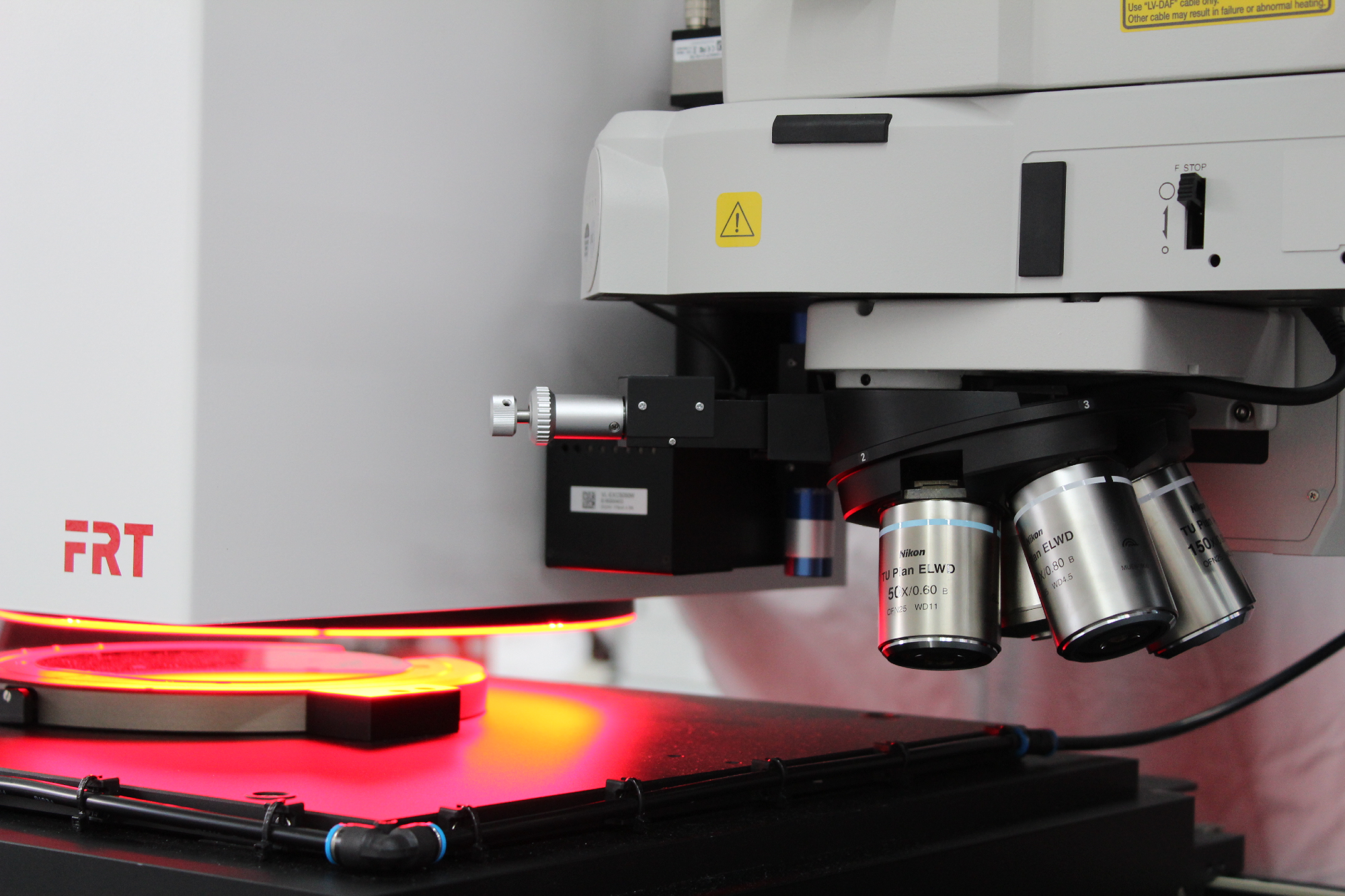
The most significant difficulty with metrology and inspection for nanosheets involves seeing very accurately vertically through multiple layers of other materials. This can also be done with high voltage contrast E-Beam, TEM, or X-Ray Spectroscopy tools, but these technologies are unsuitable for high-volume manufacturing due to low throughput and/or destructive test regimes.
At the SPIE Optics and Photonics conference, we learned that Onto uses a spectral ellipsometer and a suite of in-house software to generate complex 3D models of the vertically stacked nanosheets. While spectral ellipsometers have historically been used for thin film measurement, Onto has extended this form of optical metrology and inspection to 3D structures.
This is something KLA’s spectral ellipsometry tools cannot do well due to their lack of advanced 3D modeling software. Even if they catch up on software, Onto’s tools are generally cheaper due to their less expensive service contracts. Furthermore, this advantage of incumbent hardware/software cannot be understated. Based on our sources, they are already the POR provider for this type of tool for all 3 leading-edge fabs. This becomes a sizable moat as TSMC, Samsung, and Intel can build their tools for characterization on top of the base layer from Onto. Replacing that base layer it would require revalidation and retesting the new offering with all existing uses, applications, and processes. This is a horribly expensive task and frankly a waste of engineering effort given how much more important engineering the next process node is.
An engineer at one of these firms told us that it accelerates their learning time by achieving a higher sampling frequency and allowing them to iterate more quickly on tweaking process recipes.
This type of tool also has the potential to be used for 3D DRAM architectures. Our sources also indicate that Samsung is an early adopter of this tool for their pathfinding and development of 3D DRAM, which is fully underway. This tool is also being used in 3D NAND.
Onto has created a tool superior to KLA’s due to its advanced physics and AI-based modeling. This tool is at all 3 major logic customers and will cause market share to increase on gate all around nanosheet process technology. Investors should note that the logic opportunity alone could represent more than $400M annual revenue in 2025, with the potential to grow beyond due to 3D DRAM.
By Dylan Patel, source https://semianalysis.substack.com/p/how-onto-innovation-is-gaining-market


