For years, researchers developing microelectromechanical systems (MEMS) sensors have aimed to create a solution that would easily integrate MEMS sensing structures with the required signal conditioning to expand their applications. In the 1980s, analog circuitry and bulk micromachining were used for pressure sensors, but when automobile manufacturers required accelerometers as crash sensors in the 1990s, surface micromachining was used to create capacitive accelerometers with complementary metal-oxide-semiconductor (CMOS) signal conditioning.
Today, surface micromachining has become the go-to for the lowest power consumption and smallest structures, allowing for a range of sensor devices, such as accelerometers, gyroscopes, and pressure sensors. These devices interface with microcontrollers that use CMOS circuitry for signal conditioning and conversion.
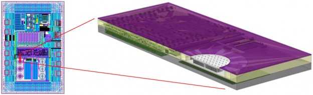
However, there has yet to be a significant advancement in wafer fab processes capable of simultaneously creating MEMS structures and CMOS circuitry without adding complexity to the CMOS process. Nanusens, a UK-based sensor company, appears to have found a solution. Using patent-pending techniques, they produced MEMS sensor structures and detection circuitry concurrently within a chip using standard CMOS processes. By employing a hydrogen fluoride solution, part of the silicon oxide was etched away in the back end of line (BEOL) of a commonly-used CMOS process in wafer-level chip scale packaging (WLCSP), allowing for the creation of the MEMS device. A bottom metal plane and a top metal plane with an array of small holes enabled the hydrogen fluoride to get inside the MEMS cavity. The resulting devices reportedly have a high yield, performance, and reliability, while minimizing processing steps and costs. The ultrafast digital detection circuitry, which switches off in 3 microseconds, leads to a sub-microampere current consumption on the 180nm test chip, making it significantly more energy-efficient than current devices on the market. This process can be used for a range of devices, such as microphones, RF switches, and tunable capacitors.


