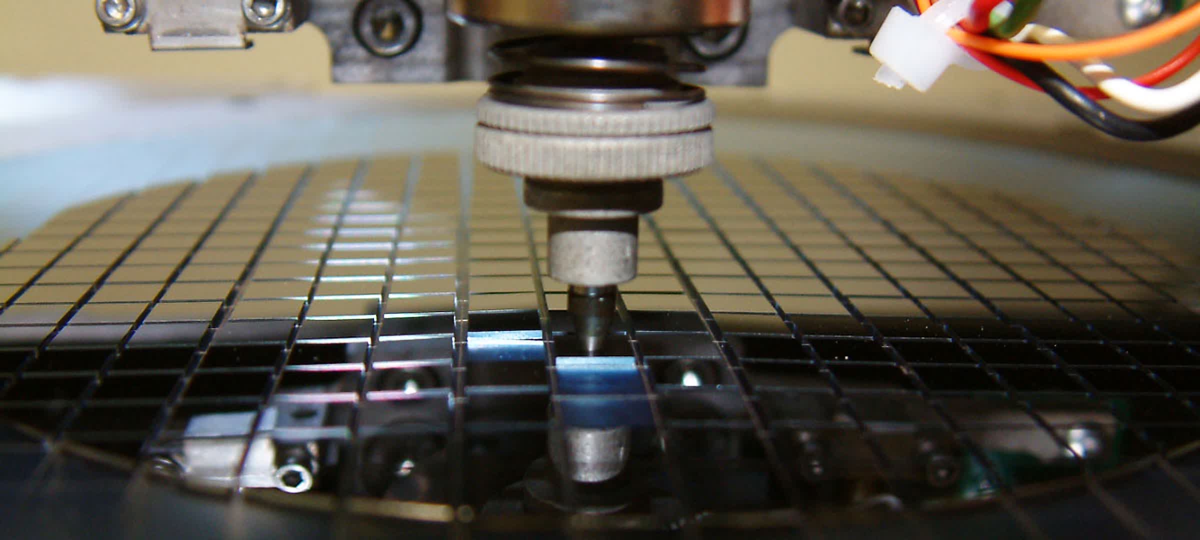
In May last year, Samsung Electronics demonstrated samples of 3nm products to US President Joseph Biden during his visit to South Korea and by the end of June the company had established mass production and began shipping the advanced chips to one of its Chinese customers. Since then 3nm products yields have risen remarkably. Now as the quality level in the production of 3nm chips on the Samsung fabrication line has “reached perfection” the company is moving at full speed towards the development of the second generation of 3nm technology.

To recap, Samsung was the first in the world to combine the structure of transistors with surrounding gate (GAA) and 3-nm lithography. Competitor TSMC launched 3nm products only late last quarter and continues to use the better-studied FinFET transistor structure. Apple is expected to be TSMC's first 3nm customer.
Rumors have attributed TSMC to achieving an impressive 85% yield rate on 3nm products, but Korean industry sources question the plausibility of such claims. In their opinion, the real rate of yield of TSMC products at this stage of the life cycle of the 3-nm process technology does not exceed 50%. Rumors also attributed to Samsung itself the existence of problems with a high level of defects in the early stages of mastering the 3nm process technology. Then it was reported that only every tenth of the manufactured chips passes the quality control procedure. Things should be much better now.
In November information appeared that NVIDIA, Qualcomm Technologies, Google, IBM and Baidu would become Samsung Electronics customers for 3nm products. As of the end of September last year, Samsung, according to TrendForce, occupied 16.4% of the market for contract chip manufacturing services, while TSMC owned all 53.4% of this market.


