Taiwan Semiconductor Manufacturing Co. (TSMC) and Samsung Electronics are engaging in a fierce competition to develop cutting-edge technology for the global foundry (semiconductor consignment production) industry. The two companies, which are ranked first and second in the industry, are currently working on the 2-nano process, following the 3-nano process.
According to foreign media and industry sources, TSMC has decided to construct four 2-nano process fabs in Taiwan's Hsinchu area, also known as Taiwan's Silicon Valley. The cost of building the four factories is expected to reach about 80 trillion won in Korean currency, and TSMC plans to start operating the new plant in 2025 at the earliest.
TSMC is also collaborating with major partners in the 2-nano process. The company is strengthening cooperation with Nvidia, Synopsys, and ASML in the field of lithography, which engraves circuit patterns on wafers.
TSMC's move to accelerate the development of the 2nm process is seen as an attempt to widen the technological gap between the company and Samsung Electronics, as advanced processes become increasingly important in the foundry field.
Currently, both companies' state-of-the-art foundry processes are at the 3-nm level. Samsung Electronics began mass production of the 3-nano process in June of last year, about half a year ahead of TSMC, and TSMC also started mass-production of the 3-nano process in December of the same year.
This is the first time that TSMC has fallen behind Samsung Electronics in advanced processes. Samsung Electronics also announced that it plans to start the 2-nano process in 2025, the same year as TSMC.
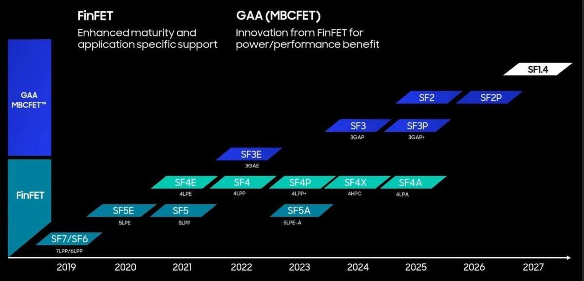
Starting with the 2-nano process, the competition in 'GAA (Gate All Around),' a next-generation technology for cutting-edge processes, will begin in earnest. The GAA technology is a form in which a gate surrounds four channels through which current flows in a transistor constituting a semiconductor. Compared to the existing FinFET structure that covers only three channels, the area of the gate is wider, so it can overcome the performance degradation of the transistor due to process miniaturization.
Unlike TSMC, which applied 'PinFlex' technology to improve the existing FinFET technology to the 3-nano process, Samsung Electronics introduced GAA technology from the 3-nano process mass-produced last year. It is interpreted to strengthen technological competitiveness in pursuit of TSMC.
Both companies are expanding their investments in advanced foundry processes. TSMC recently announced that it would increase its research and development (R&D) spending to NT$200 billion this year, an increase of about 20% from last year. Samsung Electronics spent 53.12 trillion won in facility investment last year, an increase of 10.1% from the previous year, of which 90%, or 47.87 trillion won, was invested in new and expanded semiconductor businesses. This year, the company plans to continue investing in R&D to secure competitiveness in next-generation semiconductor technology.
Samsung Electronics recently announced a mid- to long-term plan to invest 300 trillion won over the next 20 years to build a high-tech semiconductor cluster in Yongin, Gyeonggi-do.


