It is known that in the Japanese prefecture of Kumamoto, by the end of 2024, a joint venture between TSMC, Sony and Denso will start operating, which will produce semiconductor components on orders from the last two companies. Sony will build another one next to this enterprise, which will produce image sensors based on the chips that it will receive from the partner.
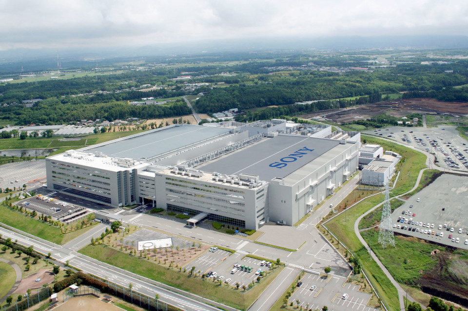
Sony's new sensor manufacturing facility in Kumamoto Prefecture will be located next to the existing one. When a joint venture with TSMC and Denso goes live next door, Sony is already set to receive image sensor chips in 2025 for further testing and packaging at its new facility. The Japanese giant has already notified its suppliers and partners about these plans. The image sensor production scale at the new facility will be adjusted according to the market situation. According to Japanese media, Sony is ready to invest up to $5.8 billion in the construction of the new enterprise.
Sony's existing facility in Kumamoto produces image sensors for a wide range of applications, from smartphones and vehicles to industrial equipment and video surveillance systems. As of April this year, it employed 3,300 people. It is Sony's largest semiconductor manufacturing facility. The corporation itself occupies about 44% in the world market of image sensors moneywise, which allows it to be considered a leader, competing with Samsung Electronics and its market share of 18%.
Stabilization and even a slight decrease in demand for smartphones does not frighten Sony, since it relies on increasing the specific number of image sensors in older smartphones. Additional demand is created by segments of automotive electronics and industrial equipment, the automation of which implies the active use of machine vision systems. All this allows Sony to justify the construction of a new facility for the manufacture of image sensors.


