With 10 times higher breakdown electric field than silicon, high electron mobility, and the ability to operate at higher junction temperature, GaN semiconductors are poised to play a significant role for the next decade's technology revolutions. At mmWave frequencies, GaN-on-silicon amplifiers excel versus alternative solutions such as Si CMOS, GaAs pHEMTs, or SiGe devices.
The inroads being made by gallium nitride (GaN) technology into the 5G world are good news for everyone concerned. However, an important aspect to making mmWave 5G available and accessible to all is the development of high-power, high-linearity mmWave power amplifiers.
Today’s approaches to such amplifiers are throttling 5G due to their inability to deliver the higher linearity and efficiency needed to solve uplink issues facing mmWave frequencies, which do not propagate nearly as far as microwave signals. Seeing an opportunity to catalyze change, Finwave is now emerging from stealth mode to unveil its next-generation 3D gallium-nitride (GaN) technology.
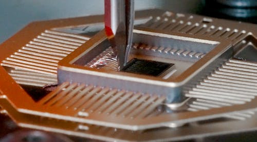
Finwave co-founders Prof. Tomas Palacios and Dr. Bin Lu first teamed at MIT to invent several of the foundational technologies for Finwave, including a novel type of GaN transistor based on a FinFET architecture. After being spun out of MIT, the company spent several years developing the technology further for manufacturing in the standard silicon CMOS fabs. By 2020, Finwave demonstrated the first GaN FinFETs fabricated with 8” silicon CMOS tools.

Finwave’s 3DGaN technology is said to significantly improve linearity, output power, and efficiency in 5G mmWave systems while reducing costs for carriers. By leveraging high volume 8” Si CMOS, Finwave’s devices benefit from both the cost model and scalability of silicon technology. “The combination of the outstanding electrostatic control and linearity of the GaN FinFET structure, with the cost model of silicon, and the scaling ability of state-of-the-art 8” and, in the future, 12” fabs makes 3DGaN a true game changer,” commented Palacios.
For more information, visit the company website.


