Scientists in China have made breakthroughs in the creation of flexible solar cells. They have used foldable crystalline silicon (c-Si) wafers instead of conventional ones to create solar cells using heterojunction (HJT) cell technology which has been shown to be ideal for flexible solar cells. The research group behind this study includes scientists from China's Tongwei (TW), the Changsha University of Science and Technology, Southwest Petroleum University, Soochow University, and Beihang University. The study showcases a promising future for the creation of flexible solar cells using foldable silicon wafers with blunted edges.
The study, published in the journal Nature, reported that using HJT cell technology eliminates edge warping caused by inner stress during the solar cells firing process. The scientists used blunting treatment, rounding the edges of the wafers to prevent chipping and cracking from processing.
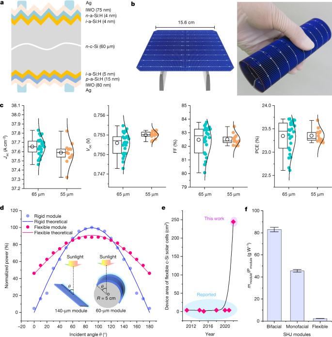
The Czochralski n-type c-Si wafers that were used ranged from 65 μm to 55 μm in thickness. Textured wafers were created by the application of a 2.1-vol% alkali water solution at 80 C, forming microscale pyramids on the surfaces. Before the cells were created, the researchers cleaned the wafers, removing organics and metal ions, and etching the surface oxide. Two cells with thicknesses of 65 μm and 55 μm were produced, with a power conversion efficiency of 23.31% and 23.35% respectively.
The team then applied an anti-reflective coating based on magnesium fluoride (MgF2) on the cells to increase their efficiency to 24.50%.
The scientists revealed that using a 60-μm wafer could reduce production costs by approximately 29%. They further reduced the levelised cost of energy by around 39% at the solar cell level. The flexible technology developed in this study has shown to be a remarkable achievement compared to other current flexible cell techniques created using cost-effective materials.


