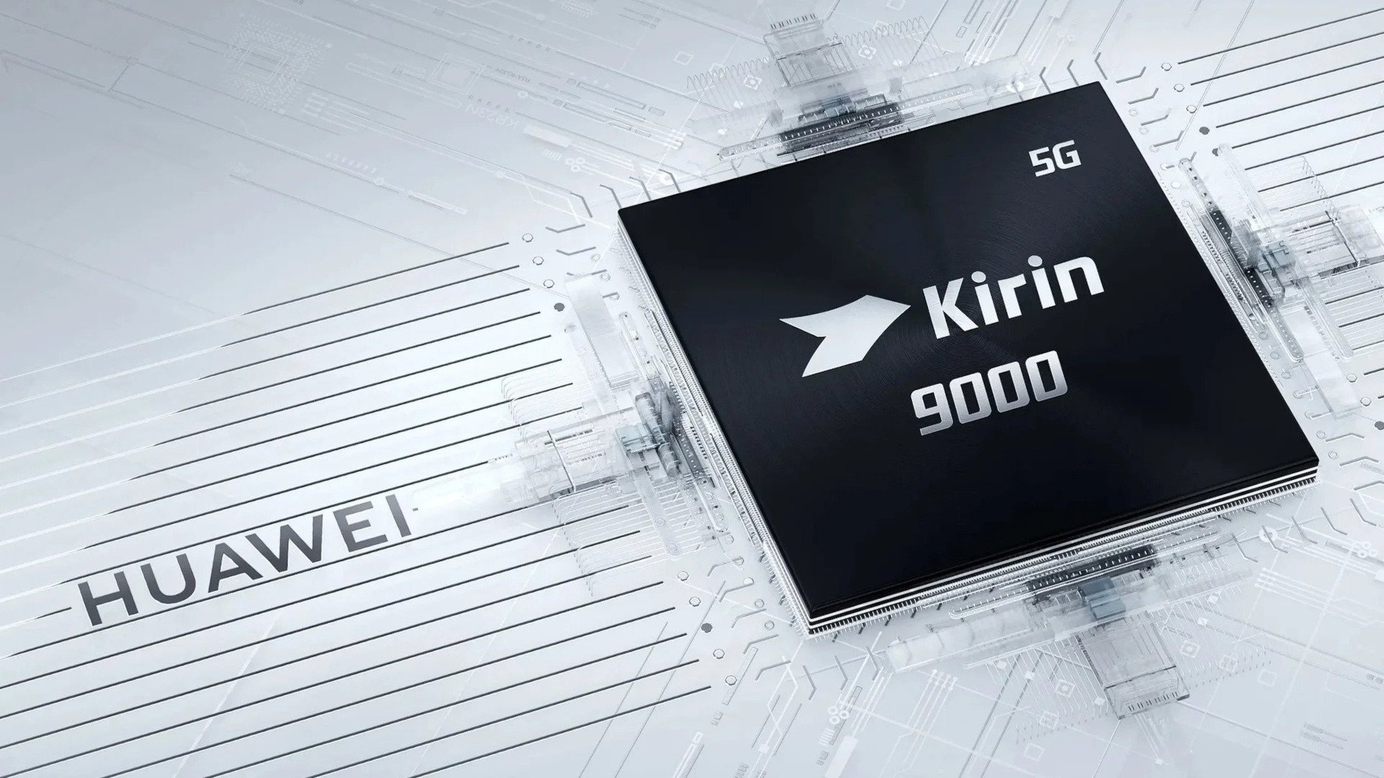
According to a report by TechInsights, Huawei's Kirin 9000S system-on-chip (SoC) powering the new Mate 60 Pro smartphone is rumored to be manufactured by China-based SMIC using their 2nd generation 7nm-class fabrication process and stacking. The SoC is reported to feature CPU and GPU microarchitectures developed in-house by Huawei's HiSilicon. It's important to note that all information about the Kirin 9000S is unofficial at this time.
The Kirin 9000S SoC appears to be quite complex, with four high-performance cores (one running at up to 2.62 GHz and two at up to 2,150 MHz) and four energy-efficient cores (up to 1,530 MHz). These cores are based on Huawei's own TaiShan microarchitecture, which is still believed to be found on the Armv8a ISA. The SoC also includes the Maleoon 910 graphics processing unit operating at up to 750 MHz.
The CPU and GPU cores in the Kirin 9000S run at relatively low clocks compared to Arm's cores featured in previous generations of HiSilicon's SoCs. This lower frequency can be explained by the fact that SMIC is producing the new SoC using their unannounced 2nd generation 7nm fabrication process. This could potentially be a significant breakthrough for SMIC, Huawei, and China's high-tech industry. It's worth noting that while TechInsights refers to this technology as SMIC's 2nd generation production node, state-controlled Global Times claims that SMIC uses its 5nm-class manufacturing technology to produce the SoC. However, it seems that these two names describe the same thing, which was once known as SMIC's N+2.
In 2020, SMIC briefly mentioned its N+2 manufacturing technology, which appeared to be an evolutionary step of its N+1. Chinese analysts also labeled N+2 as SMIC's 5nm-class production node about a year ago. Although SMIC has not confirmed that they produce chips on 7nm or 5nm-class nodes, there are independent proofs from TechInsights that SMIC produced MinerVa Semiconductor Bitcoin mining ASICs on their 7nm-class N+1 technology. Additionally, SMIC's Twinscan NXT:2000i deep ultraviolet (DUV) lithography scanners are capable of making chips on 7nm and 5nm technologies, indicating that the company may have developed a 5nm-class fabrication process. However, it's important to note that to achieve the desired features on a 5nm-class node or refined 7nm-class process technology, SMIC would heavily rely on multi-patterning, an expensive technology that affects yields and costs. Therefore, the economic efficiency of SMIC's 5nm-class technology is likely lower compared to market leaders like Intel, TSMC, and Samsung Foundry.
Another notable detail about the Kirin 9000S is its reported use of stacking technology. While Global Times did not elaborate on how the stacking is used, it is speculated that the modem IC is stacked on top of the CPU+GPU IC to save space on the motherboard or to simplify production by disaggregating some logic. Advanced packaging technology such as stacking represents a breakthrough for SMIC and/or Huawei's HiSilicon.
Huawei's HiSilicon, China's most successful chip designer, previously relied on TSMC's leading-edge fabrication technologies. However, due to Huawei's loss of access to American technologies in 2020, HiSilicon was no longer able to collaborate with TSMC. It is believed that Huawei has assisted SMIC in advancing their fabrication processes, and the Kirin 9000S is potentially the first outcome of this collaboration.


