The study conducted by Rachel A. Nye and her team at imec, KU Leuven, and North Carolina University has made significant strides in the area-selective deposition (ASD) of TiO2 films in the manufacturing of nanoelectronics. This is a critical process used by various industries, from medicine to engineering, who rely on precise and effective nanoscale production techniques. The research team has successfully implemented the passivation + deposition + etch supercycle process, which has yielded unprecedented uniformity and selectivity in film deposition on SiO2/TiN line/space patterns.
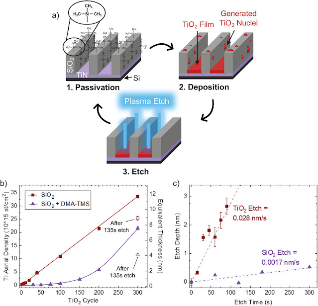
The researchers, in their quest to improve uniformity and precision, leveraged the unique properties of the DMA-TMS inhibitor, resulting in a 2× improvement in film thickness during atomic layer deposition (ALD) of TiO2. The film thickness deposited was approximately 8 nm, with uniformity as high as 88% and 100% selectivity on nanoscale patterns. The results were quite remarkable, with lower defectivity on pattern sidewalls, top surfaces, and corners, compared to earlier reports.
One of the key findings of this study was the realization that pattern-dependent uniformity is crucial. This emphasizes the importance of understanding and optimizing processes at a specific feature scale. The researchers anticipate that through further refinement, the uniformity of the films will become even better as feature sizes continue to shrink.
The research shows thativation, deposition, and etch parameters are essential in achieving unmatched uniformity and selectivity. Refining these foundational parameters can significantly impact nanoscale ASD while promoting improved control over the process.
This groundbreaking research opens up a wide range of applications for TiO2 films in nanoelectronics, including antireflection coatings, sensors, photocatalysts, and etch-resistant layers. The results of the research also provide valuable insights into the quantification of uniformity and selectivity in nanoscale patterns. This will serve as a benchmark for future advancements in nanoscale ASD, which will significantly transform design and fabrication of electronic devices on an industrial scale.


