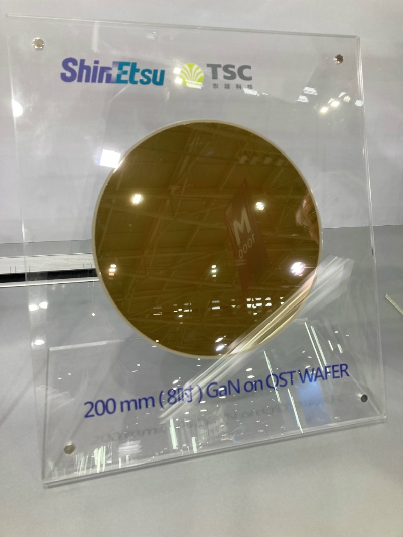
Shin-Etsu Chemical, a Japan-based company primarily involved in the chemical industry, has recently announced its plan to significantly expand the sale of QST substrates to drive the widespread adoption of GaN-based power devices. The company is also willing to provide substrates grown on gallium nitride (GaN) on request, manufactured at its own sites. Currently offering substrates with diameters of 6″ and 8″, Shin-Etsu is actively developing 12″ diameter substrates to meet market demand.
The company believes that the market for GaN is poised for significant growth due to its potential to address the increasing need for energy conservation and high-performance capabilities, especially in advancing mobility technologies such as autonomous driving, 5G communication, and deeper digitalization.
QST Substrate Technology (QST) was exclusively licensed to Shin-Etsu in 2020 by Qromis, a fabless firm based in Santa Clara, California. QST is a crucial composite material substrate designed to facilitate the growth of GaN power devices. This material plays a vital role in enabling the widespread adoption of high-performance and energy-efficient GaN power devices. With the licensed manufacturing of QST, Shin-Etsu has expanded its substrate offerings, which now include silicon-on-insulator (SOI) wafers and GaN-on-silicon wafers, in addition to conventional silicon wafers for power and high-frequency semiconductors.
The QST substrate is engineered to possess a coefficient of thermal expansion (CTE) that matches that of GaN, thereby allowing for the growth of thick GaN epitaxial layers with a large diameter and excellent quality. This technology is expected to find utility in power devices, RF devices (including 5G and future 5G networks), and MicroLED expansion for MicroLED displays.
Gallium nitride is a wide bandgap (WBG) semiconductor with outstanding properties, including higher operating voltage than silicon, lower power losses, smaller footprint, ability to operate at high temperatures, reduced heat generation, and higher switching frequencies than silicon. However, the widespread commercialization and adoption of GaN can be hindered by high manufacturing costs, performance improvement challenges, and enabling new applications.
QST substrate technology addresses these challenges by allowing scaling to 6”, 8”, 12” diameter and beyond, growing thick GaN from a few microns to bulk-like thickness on all wafer diameters, and manufacturing devices ranging from discrete to monolithic and eventually ICs with specially engineered layers. Additionally, the process and integration technologies demonstrate compatibility with existing silicon fabrication facilities, negating the need for expensive developmental efforts.
Shin-Etsu Chemical has continuously enhanced its QST substrates, including improvements to mitigate flaws arising from the bonding procedure and the availability of template substrates with tailored buffer layers to allow consistent epitaxial growth.
The company has achieved significant milestones, such as growing GaN with a thickness beyond 20 μm utilizing QST substrates and developing power devices with a breakdown voltage of 1,800V. A successful collaboration with Oki Electric Industry has resulted in the development of a technique for the exfoliation of GaN from QST substrates using Crystal Film Bonding (CFB) technology, enabling the bonding of GaN to substrates composed of diverse materials. This approach aims to contribute to the progress of vertical power devices.
Shin-Etsu Chemical will offer QST substrates and GaN grown QST substrates to companies engaged in GaN device manufacturing. Meanwhile, Oki Electric Industry will deliver its CFB technology through collaborative partnerships or license agreements, with the goal of advancing vertical power devices.


