Saxony and Sweden actually have a lot in common, Dr. Jonas Sundqvist is convincing: The school system in GDR times reminds him of the Swedish one, the idea of learning together and the like. Only really big chip factories and big clean rooms, Sweden just doesn't have them - and that's the main reason why Dresden has become a second home for the semiconductor expert Sundqvist: For more than two decades he worked in the big chip shops and research forges of "Silicon Saxony", has a Partly shaped the location.
Today, from his living room in the so-called "Schwedendorf" near the television tower, he runs his new, own semiconductor company " Alixlabs ", which he founded together with fellow countrymen in Lund, Sweden. It specializes in new etching technologies that could one day pave the way for Europe's microelectronics into the world of ultra-fine chip structures below ten nanometers (millionths of a millimeter). No wonder that he and his colleagues chose Dresden, the largest European circuit production site, to bring their new technology to market maturity.
“I then looked around Europe for a job. Germany wasn't actually on my list at all.” In 2003, therefore, he hesitantly followed the call of the former Siemens subsidiary Infineon to come to Dresden. "I had a completely wrong image of Dresden," he says. "Everyone told me that the British and Americans completely destroyed everything there in the war and that the city is still a complete wasteland to this day. The wow effect was all the greater when, after the job interview at Infineon, I was driven around here in a Mercedes and really got to see the city.”
In the years that followed, he helped Infineon to set up the ALD technology for particularly conductive "High-K" materials, which Intel and Samsung were already using, in the Dresden chip factories for the so-called "dRAM" memory on a large scale. "Back then, Infineon gradually tested all the suitable systems in Dresden," says Sundqvist.
Shortly after Infineon spun off its memory chip division, the atomic layer expert also moved to Qimonda in the neighboring building in 2006, where he researched internationally groundbreaking semiconductor technologies and met his future wife there. "It was a very interesting job back then and I was highly motivated because we were at the forefront of technology and worked with many international partners. I would estimate that we at Qimonda were about the same technologically as Samsung at the time, and even better in some areas." The close cooperation with the Dresden University also helped: "We often first tested new materials in the clean rooms of the TU and Then the first small series started up in Qimonda’s pilot clean room in building 48.”
Then came 2008 and the big chip crisis. "We were all pissed off at the time that the federal government and the EU hadn't seen the systemic importance of Qimonda for Europe." he is firmly convinced. “By now, Berlin and Brussels have long recognized how important leading-edge chips are for car production and many other industries. Today would be different. But back then, the federal government preferred to save Opel and let Qimonda go bankrupt.”
In the meantime, there has been a clear change of attitude in Berlin and Brussels: "Since cars have become mobile smartphones, and since autonomous and networked driving has been the talk of the town, microelectronics has taken on a whole new status for the federal government," says Sundqvist. “That is why it has become so important to locate TSMC, Intel or Samsung in Germany. There is always concern about what will happen if something happens to Taiwan.” Since then, the federal and state governments have been pouring millions and billions in subsidies into new chip factory settlements, expansions and research programs, be it for Intel , Infineon , Globalfoundries , Wolfspeed , Bosch, X-Fab or others.
After the memory chip giant went bankrupt in 2009, Sundqvist – like so many other Qimondians – initially applied to solar companies in Saxony. There, however, the technological challenges were far less than at an international memory chip manufacturer and the wages were noticeably lower. The semiconductor expert first switched to the Belgian electronics research center IMEC for a short interlude and then to the Fraunhofer nanoelectronics center CNT, which was just realigning itself to Globalfoundries orders. However, when it became clear that Globalfoundries in Dresden would remain stuck with the 28-nanometer generation and would not go along with the next international steps towards seven nanometers, the chemist looked around again for new challenges.
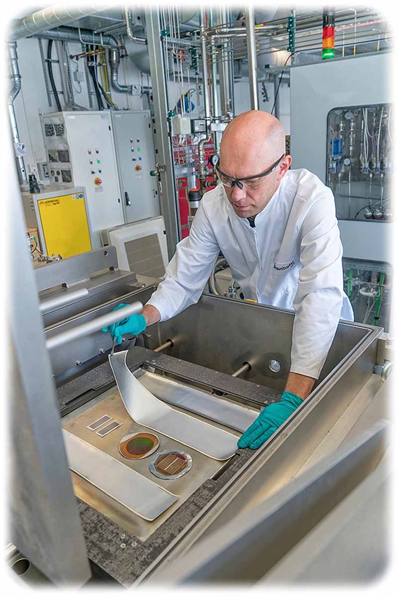
In the years that followed, he researched thin-film technologies at the TU Dresden and at the Fraunhofer Ceramics Institute IKTS in Dresden . And at the University of Lund, together with other chemists and semiconductor experts, he developed a technology not only to deposit atomic layers for chips, but also to create structures a few nanometers in size through atomic layer etch pitch splitting (APS). . Normally you need extreme ultraviolet exposure (EUV) that costs more than 100 million euros.from the Dutch sole manufacturer ASML. But Jonas Sundqvist's team was soon convinced: the APS method is a real alternative and could possibly help Europe's semiconductor industry to catch up with Samsung, TSMC and Intel in terms of structural technology. And so the Swedes founded the company " Alixlabs " in 2019, which now wants to take the process to mass production in Dresden.
According to Alixlabs, the process has so far worked on a laboratory scale down to two nanometers. "The ecosystem here in Dresden offers us the best opportunities to quickly transfer our process from the laboratory to the factory scale," emphasizes Sundqvist. “The location has become even stronger and broader in recent years. And I see it as my personal task to establish long-term high-tech cooperation between the growing clusters of southern Sweden and Saxony.”
He is now planning to set up a subsidiary in Dresden to promote the transfer to the large chip factories. The Alixlabs workforce in Sweden and Saxony is to gradually grow over the next few years to initially 30 employees. From the turn of the year 2026/27, Sundqvist wants to have the etching process so far that the first customers can start up these systems in large chip factories.


