When building new facilities in Ohio, Intel made no secret of the fact that it will be serving third-party customers with advanced 18A (18 angstroms - 18 tenths of a nanometer) technology, and US defense-related customers will be among the first to receive their orders. The company also plans to arrange packaging and product testing for such customers in Arizona.
This summer, US Department of Defense officials complained that up to 98% of the microelectronic products required by the department were produced or tested in Asia. Intel will try to solve this problem by establishing a semiconductor testing and packaging line for the US Department of Defense at its existing facilities in Arizona for the foreseeable future. The agency buys $3 billion worth of chips annually, Randhir Thakur, president of the Intel Foundry Service (IFS) division, explained in an interview with EE Times, and the company has already signed a $250 million contract under which Intel and the defense customer will be engaged in the development of advanced semiconductor components.
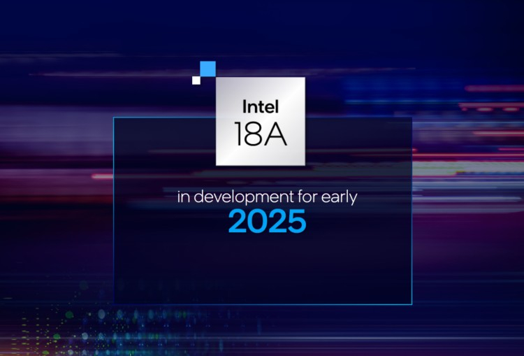
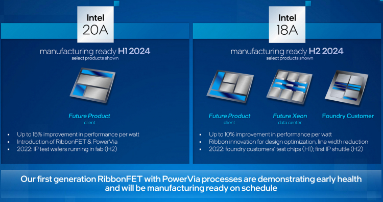
Intel intends to leverage the agency's SHIP ecosystem, which allows disparate computing components to be integrated into a single package. The US Department of Defense will be the first Intel customer to receive 18A semiconductor chips from the company in the second half of 2024. They will already use a gate-all-around (GAA) transistor structure.
IFS clients already include MediaTek, Amazon and Cisco, and in the first year of Intel's contract business they brought in about $800 million in revenue. This is not much compared to the $56.9 billion received by TSMC last year, but Intel is at the very beginning of this path. It is noteworthy that for large customers like MediaTek, Intel is going to provide "inviolable quotas" that guarantee stable production for the client even in the conditions of high demand for the company's services.
The acquisition of Israeli company Tower Semiconductor will add to the IFS ecosystem a network of facilities located in Israel, Europe, the United States and Japan, which together generated about $1.5 billion last year. Intel's business will benefit from these assets in the automotive and metaverse, as it will enable a wide range of different sensors to be released at optimal cost.
Developer Toolkit version 0.9 is now available to IFS customers to release products based on the Intel 16 process. In the case of Intel 18A technology, the toolkit has reached version 0.5, indicating that it is in the exploratory phase, although process development is still in full swing. According to an Intel representative, the 18A process technology is comparable in its parameters to the well-known 2nm process.
To become a US defense contractor, Intel must go through a complex and lengthy security certification process, but holding such a certification would automatically increase its credibility with other customers. One of the steps to build confidence will be the establishment of a chip packaging and testing line in Arizona, since now similar operations with Intel products are carried out either in Malaysia, or in China or Vietnam. Intel currently employs six different chip packaging companies, distributing orders to 18 locations.
Source https://www.eetimes.com/intel-foundrys-no-1-customer-u-s-dod-targets-gaa/


