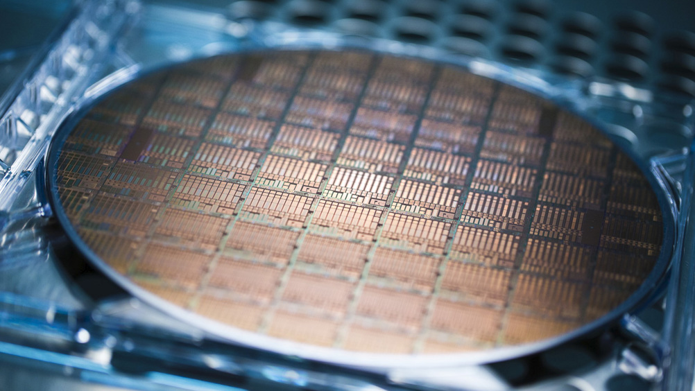
CEA-Leti and Intel have announced a project to develop layer transfer technology for 2D TMDs on 300mm wafers to extend Moore's Law beyond 2030. The joint research aims to create a viable layer-transfer technology for high-quality 2D materials to enable their use in future microelectronic devices. The two-dimensional layered semiconductors may replace traditional silicon-based transistors because of their enhanced electrostatic control, innate sub-1nm transistor channel thickness, good carrier transport, and mobility, and their suitability for high-performance and low-power platforms.
Moore's Law is a fundamental and enduring idea that has shaped the evolution of computer technology and is seen as the foundation of the digital age. The law states that the number of transistors on a microchip doubles approximately every two years, leading to exponential growth in performance and reduction in cost. The ability to maintain this growth rate over more than 50 years despite daunting technical challenges has been a remarkable achievement of the semiconductor industry.
However, the physical limits of transistor scaling are being approached, making it increasingly difficult to keep pace with Moore's Law. Current transistors are typically around 5 nanometers (nm) in size, but fundamental physical limits restrict feature sizes to around one nanometer. Beyond that, quantum mechanical effects make it difficult to control the flow of electrons.
To continue scaling transistors beyond this limit, researchers are exploring new materials and structures that could enable smaller and more efficient devices. One promising solution is the use of two-dimensional layered semiconductors, such as transition-metal dichalcogenides (TMDs), which could ultimately replace traditional silicon-based transistors.
TMDs are layered materials that are only a few atoms thick and exhibit unique electrical and optical properties that make them promising for future electronics. They are made up of two or more elements from the transition-metal group and the chalcogen group, such asolybdenum and sulfur.
2D TMDs have several advantages over traditional silicon-based transistors. They provide innate sub-1nm transistor channel thickness, which can lead to higher density and lower power consumption. They also have good carrier transport and mobility, even for atomically thin layers, and enhanced electrostatic control due to their device body thickness and moderate energy bandgap, which can lead to lower off-state currents. In addition, they can be stacked in multiple layers to form 2D-FET stacked nanosheet devices that provide even greater density and lower power consumption.
However, there are several challenges to using 2D TMDs for future electronics. One of the biggest challenges is achieving high-quality 2D channel growth, which requires high-temperature processes that can damage other materials and structures on the wafer. Another challenge is transferring the 2D material to another substrate without damaging it, which is necessary for device integration.
To address these challenges, CEA-Leti and Intel have announced a joint research project to develop a layer-transfer technology for 2D TMDs on 300mm wafers. The project aims to develop a viable layer-transfer technology for high-quality 2D materials that will enable their integration into future microelectronic devices.
Intel brings its semiconductor-and-packaging research and technology expertise to the project, while CEA-Leti provides bonding and transfer-layer expertise and large-scale characterization. The project follows a research breakthrough announced in June on a new die-to-wafer bonding technology using a self-assembly process for future chip integration.
CEA-Leti CEO Sebastien Dauvé said the project was essential to integrate 2D materials in future microelectronic devices. The transfer capability in 300mm wafers will be key to that integration. Due to their high-growth temperature exceeding 700°C and high-quality growth on preferred substrates, it is difficult to stack 2D materials as usual thin layers. Therefore, transfer holds the most promise for integrating them in future devices, and CEA-Leti's strengths in this context are its expertise and know-how in transfer development and characterization.
The joint research project is expected to last for several years and could a major impact on the future of microelectronics. By developing a viable layer-transfer technology for high-quality 2D materials, the project aims to extend Moore's Law beyond 2030, paving the way for even more powerful and efficient computer technology.


