Decades ago, making a better computer chip was as simple as using smaller transistors and narrower interconnects. However, this method is no longer effective in keeping up with the exponential pace of computing. To address this issue, researchers at ITF World 2023 in Antwerp, Belgium, proposed a new scheme called system technology co-optimization (STCO).
STCO involves breaking down chips into their functional components, using the optimal transistor and interconnect technology for each function, and then stitching them back together to create a lower-power and better-functioning whole. Imec, a Belgium-based nanotech research organization, calls this vision CMOS 2.0. While the semiconductor industry was once able to regularly produce smaller, lower-power, and faster transistors that could be used for every function on a chip, the limits of physics and economic realities have made a one-size-fits-all transistor impractical. STCO involves looking a system-on-chip as a collection of functions, optimizing each function using the process technology best suited to it, and binding them together using advanced 3D stacking. Examples of this approach can already be seen in advanced processors and AI accelerators. The roadmap for CMOS 2.0 involves continuing to shrink transistors, moving power and clock signals beneath a CPU's silicon, and ever-tighter 3D-chip integration.
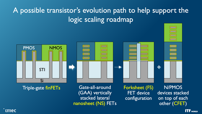
To continue scaling down devices, chipmakers are transitioning from FinFET transistors to nanosheet transistors. The complementary FET (CFET), which involves stacking two nanosheet transistors, represents the ultimate in CMOS scaling. To achieve this, they will use ASML's next generation of extreme-ultraviolet lithography, called high-numerical-aperture EUV, which provides more precise images. Additionally, backside power-delivery networks aim to remove all power delivering interconnects from above the silicon surface and place them below, which reduces power loss and frees up space for signal-carrying interconnects. Three-dimensional (3D) integration, such as wafer-to-wafer and die-to-wafer hybrid bonding, provides the highest density of interconnections between two silicon dies, but it requires that the two dies are designed together so that their functions and interconnect points align. To reach CMOS 2.0, it is necessary to take disaggregation and heterogeneous integration to the extreme by incorporating layers of embedded memory, I/O and power infrastructure, high-density logic, high drive-current logic, and huge amounts of cache memory. However, it is important to note that different systems have unique requirements and constraints, so it is necessary to discern which technologies will actually improve a system.


