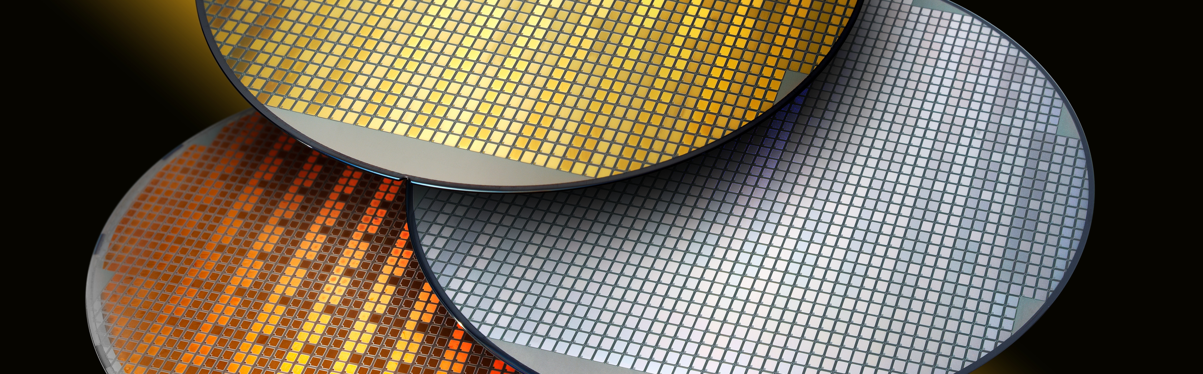
The revolution in advanced semiconductors, particularly gallium nitride (GaN) and silicon carbide (SiC), is not only transforming the lighting industry but also poised to make a significant impact in mitigating climate change by cutting greenhouse gas emissions.

GaN-based light-emitting diodes (LEDs) have rapidly captured over 50% of the global lighting market in just two decades, with LED lighting predicted to reduce electricity used for lighting by 30 to 40% in the next seven years. GaN and SiC devices are also displacing silicon-based electronics in power electronics, offering better performance and higher efficiency. The energy savings from these advanced semiconductors will be substantial, particularly in power conversion applications where wasted watts can be reduced, such as in chargers for smartphones, laptops, and electric vehicles, and in wireless base-station amplifiers. Power conversion plays a critical role in improving energy efficiency and reducing greenhouse gas emissions, as seen in the example of California where increased efficiency of refrigerators and air conditioners using power electronics has contributed to flat electricity consumption despite economic growth. The competition between GaN and SiC in various applications will likely shape the future landscape of advanced semiconductors, but both hold great promise in addressing climate change by cutting emissions and reducing energy waste.
Unleashing the Power of Next-Generation Transistors
Two critical characteristics of power transistors are speed of operation and voltage blocking capability, both of which are determined by physical properties of the semiconductor materials used in their fabrication. Speed is determined by the mobility and velocity of charges within the semiconductor, while voltage blocking capability is determined by the material's bandgap and electric breakdown field [source: "The Application of Third Generation Semiconductor in Power Industry" by Yuqian Zhang, E3S Web of Conferences, Volume 198, 2020].
Let's take a closer look at mobility, which is measured in units of centimeters squared per volt second (cm2/V·s). The product of mobility and electric field determines the velocity of electrons, and higher velocity results in higher current carrying capacity for a given amount of moving charge. Silicon has a mobility of 1,450, SiC has around 950, and GaN boasts an impressive 2,000. GaN's exceptionally high mobility is the reason it finds applications not only in power conversion, but also in microwave amplifiers. GaN transistors can amplify signals with frequencies as high as 100 gigahertz, surpassing the maximum of 3 to 4 GHz for silicon LDMOS, and even the highest 5G millimeter-wave frequencies of 52.6 GHz. With frequencies reaching as high as 140 GHz for in-room communications, the demand for bandwidth is insatiable [source: "The Application of Third Generation Semiconductor in Power Industry" by Yuqian Zhang, E3S Web of Conferences, Volume 198, 2020].
While performance figures are crucial, they are not the only criteria for comparing GaN and SiC for specific applications. Other factors such as ease of use and cost, both for the devices and the integrated systems, play a critical role. When all these factors are considered, they help explain why GaN and SiC are displacing silicon in certain applications and how their competition may evolve in the future.
Currently, SiC leads GaN in power conversion. The first commercially viable SiC transistor that outperformed silicon was introduced by Cree (now Wolfspeed) in 2011. It could block 1,200 volts and had a low resistance of 80 milliohms during current conduction. Today, there are three different types of SiC transistors available in the market, including a trench MOSFET from Rohm, DMOSs from Infineon Technologies, ON Semiconductor Corp., STMicroelectronics, Wolfspeed, and others, and a vertical-junction field-effect transistor from Qorvo.
One significant advantage of SiC MOSFETs is their similarity to traditional silicon MOSFETs, including identical packaging. SiC MOSFETs operate in a similar manner to ordinary silicon MOSFETs, with a source, gate, and drain. When the device is on, electrons flow from a heavily doped n-type source across a lightly doped bulk region before being drained through a conductive substrate. This similarity makes it easier for engineers to transition to SiC with minimal learning curve.
Compared to GaN, SiC also offers other advantages. SiC MOSFETs are inherently "fail-open" devices, meaning that if the control circuit fails, the transistor stops conducting current. This feature is crucial in eliminating the risk of short circuits, fires, or explosions due to failure. However, it comes at the cost of lower electron mobility, which increases resistance when the device is in operation.
However, despite its unique advantages, Gallium Nitride (GaN) semiconductors still face challenges in certain areas. One of the main drawbacks of GaN technology is the lack of a reliable insulator technology, which complicates the design of fail-safe devices that can fail open if the control circuit fails.
There are two options currently being pursued to achieve a normally off characteristic for GaN transistors. One option is to equip the transistor with a type of gate that removes the charge in the channel when no voltage is applied to the gate, and conducts current only when a positive voltage is applied to the gate. These types of devices are called enhancement-mode devices and are offered by companies such as EPC, GaN Systems, Infineon, Innoscience, and Navitas.

The other option is called the cascode solution, which involves using a separate, low-loss silicon field-effect transistor to provide the fail-safe feature for the GaN transistor. This cascode solution is utilized by companies such as Power Integrations, Texas Instruments, and Transphorm. (See illustration, "Cascoded Depletion-Mode GaN Transistor")
Despite the challenges in achieving a normally off characteristic for GaN transistors, the benefits of GaN technology cannot be ignored. The extremely high electron mobility of GaN is one of its main advantages. In GaN transistors, most of the current flowing through the device is due to electron velocity rather than charge concentration. This means that compared to other technologies such as silicon (Si) or silicon carbide (SiC), less charge has to flow into the device to switch it on or off, reducing the energy needed for each switching cycle and contributing to high efficiency.
Furthermore, GaN transistors are capable of switching at very high speeds, on the order of 50 volts per nanosecond, enabling them to operate efficiently at frequencies in the multiple hundreds of kilohertz, compared to around 100 kilohertz for silicon or SiC. This high efficiency and high frequency operation allows for smaller and lighter power converters based on GaN devices, as smaller heat sinks are required due to the high efficiency, and smaller inductors and capacitors can be used due to the high frequency operation.
GaN technology has gained commercial success in the markets for light-emitting diodes and semiconductor lasers due to its unique ability to emit bright green, blue, purple, and ultraviolet light. However, GaN's advantages extend beyond optoelectronics to high-power electronics, with its high electron mobility allowing for high efficiency and high frequency operation. While challenges remain in achieving a reliable insulator technology for GaN transistors, enhancement-mode devices and the cascode solution are being pursued as options to achieve a normally off characteristic. With ongoing research and development efforts, GaN is steadily gaining momentum as a promising technology for a wide range of applications in the field of electronics.
Illustrations depicting the operation of a highly advanced gallium-nitride (GaN) transistor reveal a solution to the challenge of reliable operation during control circuit failures. Known as cascoded depletion-mode, this solution involves using a low-voltage signal from a silicon field-effect transistor (FET) to control a much higher voltage on a GaN high electron mobility transistor. In the event of a control circuit failure, the FET's gate voltage drops to zero, causing it to stop conducting current and subsequently causing the GaN transistor to stop conducting as well due to the open circuit. This ensures safety by preventing current flow when the control circuit fails.
When comparing GaN and silicon carbide (SiC) devices, cost is an important consideration. Generally, SiC devices have smaller die sizes, which translates to lower costs. However, SiC substrates and fabrication costs are higher than those for GaN, and the final device costs for applications at 5 kilowatts and higher are not significantly different today. Future trends, however, are expected to favor GaN due to its relative simplicity, which may result in production costs low enough to offset the larger die size.
To be viable for high-power applications that require high voltages, GaN must develop cost-effective, high-performance devices rated for 1,200 V, as SiC transistors are already available at that voltage. Currently, commercially available GaN transistors are rated for 900 V, with some recent demonstrations of 1,200-V devices with performance comparable to SiC devices. Projections from research firm Omdia suggest that the price of 1,200-V SiC metal-oxide-semiconductor field-effect transistors (MOSFETs) will be around 16 cents per ampere in 2025. It is estimated that the lower cost of GaN substrates may result in first-generation 1,200-V GaN transistors being priced lower than their SiC counterparts by 2025, although this remains to be seen.
When considering specific applications, such as electric vehicle (EV) inverters and converters, SiC has gained early traction with major automakers like Tesla, Mercedes-Benz, and Lucid Motors using SiC devices in their EVs. However, for GaN to make inroads in this market, it will need to offer a 1,200-V device, as EV electrical systems are increasingly operating at higher voltages, such as 800 V and 900 V. The first commercial 1,200-V GaN transistors are expected to be available in 2025, and their higher switching speeds could be advantageous in EV inverters, which require fast switching to minimize high voltage and high current operation.
In addition to EV inverters, GaN is also attractive for onboard chargers in EVs, as well as phone, tablet, and laptop chargers, due to its high switching speeds and generally lower costs compared to SiC. However, for very-high-voltage power conversion applications rated at 3 kV and higher, SiC is expected to remain the dominant choice for at least the next decade. Overall, the competition between GaN and SiC in various applications will likely continue to evolve as both technologies advance and their cost-performance trade-offs become clearer in the coming years.
The Battle of Wide-Bandgap Semiconductors: A New Technological Frontier
Currently, silicon carbide (SiC) holds dominion in electric vehicle (EV) inverters and other applications where voltage-blocking capability and power handling are critical, especially at low frequencies. Meanwhile, gallium nitride (GaN) takes the lead in high-frequency performance for 5G and 6G base stations, radar systems, and high-frequency power-conversion applications like wall-plug adapters, microinverters, and power supplies.
Yet, the rivalry between GaN and SiC has just begun. As the competition unfolds in various applications and markets, one thing is certain: the environment will emerge as the ultimate winner. In the coming years, countless billions of tonnes of greenhouse gases will be avoided as this new cycle of technological advancement and rejuvenation progresses inexorably forward.


