Intel is on the verge of revolutionizing the semiconductor industry with PowerVia, an innovative approach to power delivery that necessitated a complete reimagining of chip manufacturing and testing methodologies.
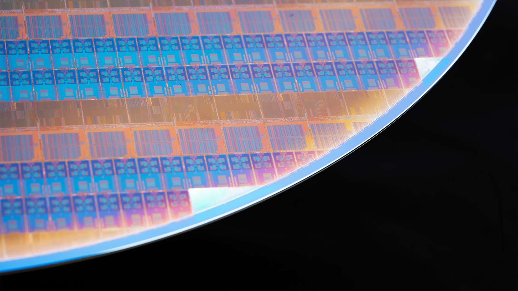
Traditionally, computer chips have been constructed layer by layer, akin to assembling a pizza. The process starts with the smallest components, the transistors, and then progressively builds up layers of increasingly larger wires, known as interconnects, to connect the transistors and various parts of the chip. Among these upper layers are the power wires that supply the chip with the necessary electrical energy.
Once the chip is completed, it is flipped over, encased in packaging that facilitates connections to the external world, and is ready for integration into a computer system.
However, this conventional approach is encountering challenges. As chip features shrink and become denser, the overlapping layers sharing interconnects and power connections create a convoluted web that hampers overall chip performance.
Ben Sell, Vice President of Technology Development at Intel and a member of the PowerVia development team, acknowledges that what was once an insignificant aspect of chip design now has a significant impact. Power and signal integrity degrade, necessitating workarounds or the injection of additional power.
Recognizing these issues, Intel and other leading-edge chipmakers are pursuing a solution known as "backside power." This entails relocating the power wires to the "back" side of the chip, beneath the transistors, while keeping the "front" side dedicated solely to interconnection.
At first glance, this approach seems obvious. So why was it not adopted earlier? There are two straightforward reasons: the old method was simpler to implement, and the associated challenges were not significant until now.
However, Intel has managed to overcome these obstacles.
Intel's backside power solution, named PowerVia, is supported by two upcoming papers to be published at the 2023 VLSI Symposium. These papers document Intel's achievement of manufacturing, testing, and demonstrating positive performance results with PowerVia. The manufacturing process itself is particularly surprising, as it departs from the traditional sequential method. For the first time, chipmaking involves a two-sided approach.
Here's how it works: Transistors are constructed first, followed by the addition of interconnect layers. Then, the wafer is flipped over, and a meticulous "polishing" process is performed to expose the bottom layer where power wires (referred to as metal layers) will be connected. Although it is called silicon technology, the amount of silicon remaining on the wafer after polishing is incredibly small.
Sell explains that after polishing, only a few thick metal layers remain, providing a direct path for power delivery to the transistors. In the realm of nanometers, "thick" equates to mere micrometers.
The advantages of this approach outweigh the increased complexity of the new process, as confirmed by Sell. For instance, the power wires consume up to 20% of the front-side real estate, and by removing them, the interconnect layers can be more relaxed. This offsets the cost of the new process, simplifying the previously challenging manufacturing flow. Consequently, the two-step flip-over process is actually cheaper than the conventional approach.
The benefits extend beyond manufacturing. The test chip, named Blue Sky Creek and based on the Efficient-core (E-core) design of Intel's upcoming Meteor Lake processor, demonstrates the effectiveness of PowerVia in addressing the problems caused by the traditional pizza-like construction method. With separate, thicker power and interconnect wires, PowerVia enhances power delivery and signal wiring, resulting in more efficient speed for the average computer user. This aligns with the promise of Moore's Law - accomplishing work faster and with lower power consumption. The second paper states, "The Intel E-core designed with PowerVia demonstrates a frequency improvement of over 5% and a cell density of over 90%, with acceptable debug times comparable to Intel 4.
Sell emphasizes that this represents a substantial frequency boost achieved simply by rearranging the wires.Debugging poses a critical challenge due to the new backside power delivery. Traditional chip-testing techniques relied on accessing the transistors in the lowermost layer. With the transistors now situated in the middle of the chip, extensive redevelopment of debugging methods was required. Sell describes the process as being accompanied by numerous concerns and hesitancy. To address this, the test chip design team intentionally introduced hidden bugs, unbeknownst to the validation team. Fortunately, they successfully detected and resolved these issues.
Significant progress has been made in developing debug capabilities over the past few years, demonstrated through the successful implementation and validation of these capabilities on Blue Sky Creek, Sell confirms.
Another noteworthy aspect of the PowerVia development process is how Sell and the Intel team devised the recipe for its implementation. PowerVia will be integrated into Intel-manufactured silicon starting with the Intel 20A node, slated for production in 2024. To isolate the development of PowerVia, they utilized the well-established transistors from the preceding Intel 4 process node and created an intermediate node that incorporated the power and interconnect design intended for Intel 20A.
While Intel's manufacturing and design teams routinely produce various test chips for experimenting with new designs and solidifying silicon processes, these chips are not typically as fully functional and complete as Blue Sky Creek. In this case, the teams needed to verify not only the feasibility of building and testing a chip using this approach but also ensure that it wouldn't introduce new issues into the final product.
One concern was the potential impact on heat dissipation. Sell explains that the traditional usage of the silicon side for heat dissipation is disrupted when transistors are sandwiched in the middle of the chip. The question arises: Will this configuration lead to significant local heating? Surprisingly, the answer is no.
Sell recalls the most astonishing aspect of this radical transformation: Despite sandwiching the transistors and implementing the extensive polishing process, the transistors closely resemble those in the Intel 4 process node.
PowerVia stands as a unique innovation without any direct competitors. According to recent reports, Intel's planned introduction of PowerVia in 2024 puts its competitors approximately two years behind in terms of backside power implementation.
"For this time period, at least," Sell confirms, "we have a highly competitive backside power delivery option."
The first opportunity to experience the manifold benefits of PowerVia will arrive next year with Arrow Lake, a next-generation Intel processor for PCs built using the Intel 20A process. With its inverted billions of transistors, Arrow Lake will operate more efficiently than ever before.


