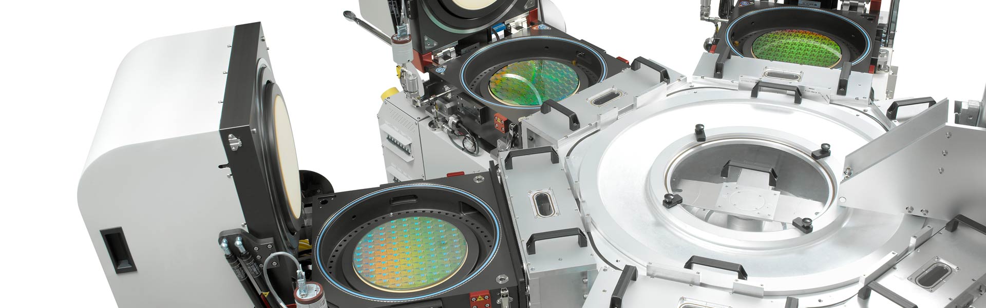
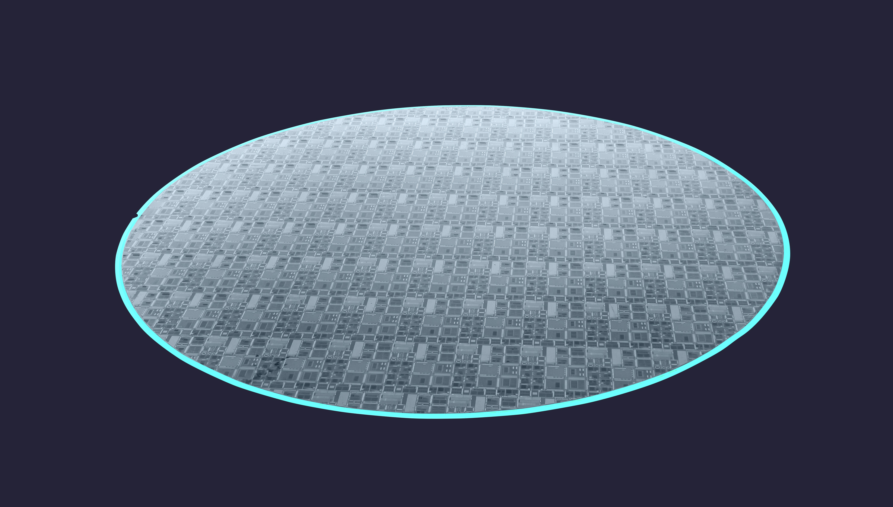
Lam Research Corp. (Nasdaq: LRCX) announced the industry's first bevel deposition solution called Coronus DX on June 20, 2023. The solution optimizes the production process of next-generation logic, 3D NAND, and advanced packaging applications. Semiconductors continually scale leading to an intricate manufacturing process with hundreds of steps required to build nanometer-sized devices on a silicon wafer. Coronus DX applies a proprietary layer of a protective film in a single step to both sides of the wafer edge, which helps prevent defects, as well as damage often seen during the production of advanced semiconductors. This protective film enhances chipmakers' yield and allows them to implement new processes for next-generation chips. Coronus DX, an addition to Lam's Coronus product line, exemplifies the company's leadership in bevel technology.
Sesha Varadarajan, Global Products Group's senior vice president at Lam Research, said that production of 3D chipmaking is expensive and challenging. The Coronus DX helps to achieve more predictable manufacturing and significantly higher yield, enabling the adoption of advanced logic, packaging, and 3D NAND production processes that were unachievable before.
Coronus DX adds critical protection during the process of integration. When repeated layers of processing accumulate residues and roughness along the wafer edge, the deposition in Coronus DX prevents defects that may cause a semiconductor device to fail. For instance, in 3D packaging applications, material from back-end-of-line can migrate, become a contamination source in future processing, and may impact wafer bonding quality. Another example is that long wet etch processes in 3D NAND manufacturing can cause severe substrate damage at the edge. This deposition provides precise and tunable protection, thereby solving common issues that may impact semiconductor quality.
Anne Roule, Head of the Semiconductor Platform Division at CEA-Leti, noted that their expertise in innovative, sustainable technology solutions helped Lam Research tackle critical challenges in advanced semiconductor manufacturing. She added that Coronus DX drives significantly higher yield, simplifying 3D integration, and allowing chipmakers to adopt breakthrough production procedures.
Coronus DX enables best-in-class precision wafer centering and process control, including integrated metrology, ensuring consistency and repeatability in the process. Coronus incrementally increases wafer yield, delivering an additional 0.2 to 0.5 percent of yield per etch or deposition step, which leads to five percent improvement across the wafer flow. This yield improvement can result in millions of extra die worth millions of dollars for manufacturers who run more than 100,000 starts per month. Coronus products are used for the manufacturing of logic, memory, and specialty devices, including leading-edge 3D devices. Every major semiconductor manufacturer uses Coronus, with thousands of installed chambers worldwide. Coronus DX is currently used in leading customer fabs globally.
Hideshi Miyajima (Ph.D.), the Technology Executive of Memory Process at Kioxia Corporation, said that improving quality in the production process via advancements like bevel technology is essential to provide next-generation flash memory at scale to customers. He added that Kioxia Corporation looks forward to continuing to work with Lam Research and its Coronus solutions for leading-edge wafer production.


