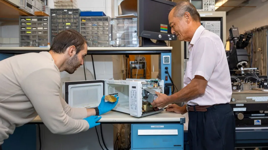
Scientists at Cornell University have been using a modified household microwave oven to help overcome a significant obstacle to practical 2nm semiconductor production. The resulting microwave annealer borrows inspiration from TSMC’s theories about microwaves and silicon doping with phosphorus. As a result, semiconductor manufacturers could push past a previous phosphorus concentration limit using the newly devised equipment and techniques.
For semiconductor processes to continue shrinking, silicon must be doped with higher and higher phosphorus concentrations to facilitate accurate and stable current delivery. As things stand, with the industry starting mass production of 3nm components, traditional annealing methods are still working effectively. However, as the industry reaches beyond 3nm, concentrations of phosphorus that are higher than its equilibrium solubility in silicon need to be ensured. As well as achieving higher concentration levels, consistency is vital in making functional semiconductor materials.
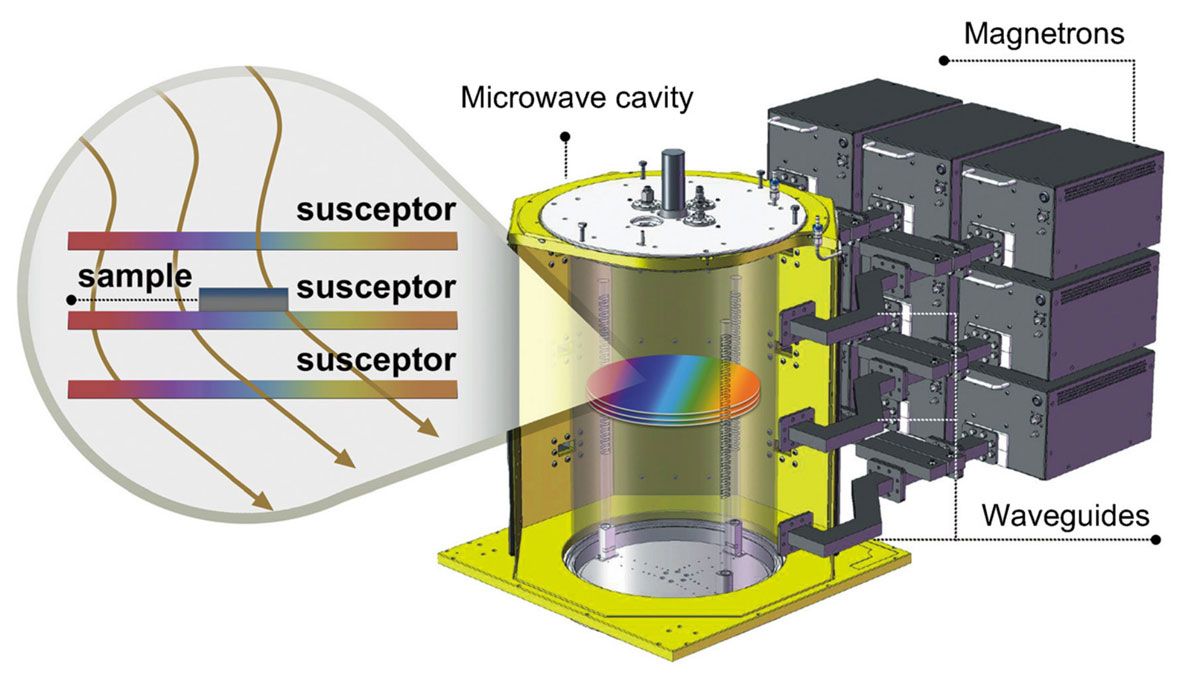
TSMC had previously theorized that microwaves could be used in the annealing (heating) process to facilitate the increased doping concentrations of phosphorus. However, microwave heating sources previously tended to produce standing waves, which are bad for heating consistency. In simple terms, previous microwave annealing devices heated their contents unevenly.
Cornell University scientists got the backing of TSMC, and the Ministry of Science and Technology of Taiwan, to conduct their research into microwave annealing. In their resulting scientific paper, shared by Cornell University earlier in the week, the scientists concluded they had “overcome the fundamental challenge for high yet stable doping above the solubility,” thanks to their advanced microwave annealing methods.
You can read in-depth about this research in the paper published by Applied Physics Letters dubbed “Efficient and stable activation by microwave annealing of nanosheet silicon doped with phosphorus above its solubility limit.” You will also note from the paper’s name that this annealing technique is good for the newest nanosheet transistor technology, where transistors are stacked in layers. TSMC has already stated it will use nanosheets at 2nm for producing gate-all-around field-effect transistors (GAAFETs).
The lead author of the paper, James Hwang, a research professor in the Department of Materials Science and Engineering, told the Cornell news blog(opens in new tab), “This new microwave approach can potentially enable leading manufacturers such as TSMC and Samsung to scale down to just 2 nanometers.” The research is going to continue and already has further funding in place.
By Mark Tyson, source https://www.tomshardware.com/news/modified-household-microwave-oven-overcomes-2nm-semiconductor-hurdle


