Over the past 70 years, chipmakers have relentlessly worked to produce smaller, better, and cheaper chips. Currently, they are preparing to mass produce chips on the 3-nanometer process node. However, the journey to achieve ever-finer circuitry on silicon almost came to a halt at the 65-nanometer threshold. It was a fortunate twist of fate involving a puddle of water that saved the day. Let's explore the inspiring history behind the immersion DUV lithography systems.
In the early 2000s, the chip industry was transitioning from lithography with argon fluoride (ArF) light sources at 193 nanometers to lithography with fluorine (F2) light sources at 157 nanometers. This shift to a smaller wavelength aimed to shrink transistors and enable more computing power and memory function on a chip. However, when calcium fluoride lenses were used in the prototype lithography systems, double refraction effects occurred, exceeding imaging specifications. It seemed lithography had hit a roadblock.
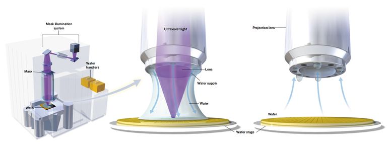
At an industry conference on 157-nanometer lithography in 2001, ASML researcher Jan Mulkens and his colleagues learned about using a layer of purified water under the lens to enhance resolution. They realized that this optical technique could extend lithography further, bypassing the challenges faced with 157-nanometer lithography. By using water as the optical fluid, all the existing optics, masks, and photoresists could still be used. This breakthrough allowed the industry to continue shrinking transistors and adhering to Moore's Law.
Jan Mulkens and his team began developing the concept of immersion lithography, focusing on the TWINSCAN platform, which allowed for accurate alignment and focus measurement. They also collaborated with ZEISS, who modified regular lenses for immersion lithography. Additionally, Philips Research contributed with their high-density optical recording technology expertise.
By 2003, the immersion team demonstrated concrete imaging results on the TWINSCAN AT:1150i prototype system. This led to the development of new lithography systems that addressed the industry's resolution struggle. In 2004, TSMC announced the first fully functional 90-nanometer node chips manufactured with early immersion systems.
In 2006, ASML launched the XT:1700Fi system, bringing immersion lithography into volume production. The system's imaging performance enabled significant resolution improvement and increased productivity. Further refinements and new systems followed, keeping up with Moore's Law.
As chipmakers aimed for even sharper imaging for smaller nodes, they experimented with multi-patterning technology. The NXT platform was developed as the successor to the compact XT platform, combining the speed of the NXT platform with the resolution of immersion lithography. The TWINSCAN NXT:1950i was introduced in 2008 for mass production of the 32-nanometer node, and subsequent systems were developed for sub-32-nanometer nodes.
Currently, the NXT platform dominates the immersion system market, with the NXT:2100i being the most recent release. The productivity of NXT immersion systems has more than doubled in the last nine years, with the capability to run over 6,000 wafers per day. Immersion lithography continues to drive innovation, with its productivity and affordability being key factors for chipmakers.
This way immersion lithography, propelled by innovations and collaborations, has played a crucial role in enabling chipmakers to continue shrinking transistors and driving the semiconductor industry forward.


