Tokyo Electron (TEL) recently announced the development of Extreme Laser Lift Off (XLO) technology by a team at Tokyo Electron Kyushu. This technology is designed to facilitate innovations in the 3D integration of advanced semiconductor devices that utilize permanent wafer bonding. Specifically, XLO is aimed at separating the top silicon substrate from the bottom substrate, both of which have integrated circuit layers, through the use of a laser.
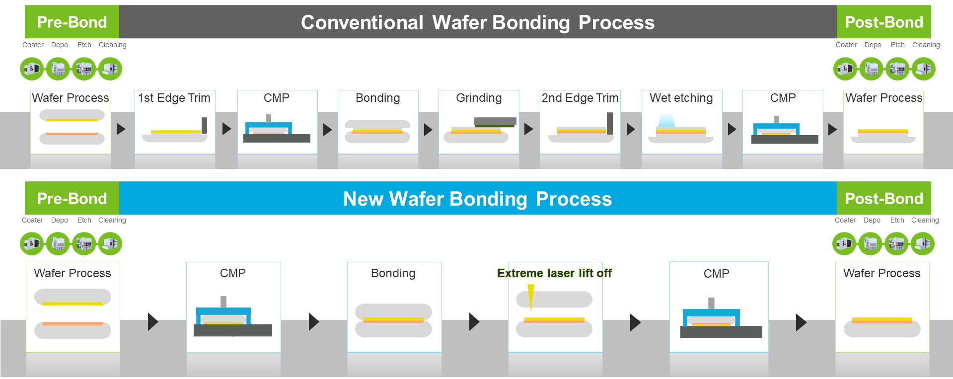
The rapid advancement of the digital society has generated increased demand for enhancements in semiconductor chip performance. Consequently, next-generation semiconductors are being developed to achieve further scaling, higher integration, and advancements in 3D integration using permanent wafer-to-wafer bonding technology. In the current permanent wafer bonding process, two wafers with integrated circuits are permanently bonded together prior to undergoing a grinding process to thin and remove the top wafer. However, concerns have arisen regarding the impact of the grinding process on yield, including issues such as stress on the wafers during grinding, delamination of films after grinding, and widening of the edge trimming area, which reduces the number of viable chips on a wafer.
TEL's XLO technology addresses these concerns by replacing the current wafer thinning and removal process, which relies on grinding, with a method that allows for the removal of the top silicon wafer without the associated yield concerns.
The Extreme Laser Lift Off technology simplifies the wafer thinning process by eliminating multiple existing steps, such as backside grinding, polishing, and chemical etching of the silicon wafer. Additionally, compared to the traditional grinding process, the XLO process does not require deionized water, leading to a substantial reduction in water consumption and the generation of drain water, thus contributing to alleviating the environmental impact. Furthermore, TEL is also working on developing a method to appropriately treat and reuse the top silicon substrate separated by Extreme Laser Lift Off, which can assist in reducing CO2 emissions from wafer fabrication.
TEL remains committed to its mission of delivering the best products and technical services and aims to continue driving technological innovation in the semiconductor industry. As the company celebrates its 60th anniversary, it perceives this milestone as a new starting point for ongoing challenges and evolution to contribute to the development of an inspirational society.


