With the aim of achieving net-zero carbon emissions, there is a growing global push for increased electrification in sectors like transportation, industry, and residential usage. To make this transition successful, it is crucial to improve the efficiency and reduce the costs associated with energy generation, transmission, and conversion. Wide Band Gap (WBG) semiconductor power devices, specifically those made from silicon carbide (SiC) and gallium nitride (GaN), have demonstrated significant advancements in power conversion efficiency and density compared to traditional silicon (Si) power devices. In this article, we will explore the potential advantages and challenges of using diamond semiconductors in future power conversion applications, with a specific focus on a new laser slicing technique.
Diamond, along with gallium oxide (Ga2O3), falls under the category of Ultra Wide Band Gap (UWBG) semiconductors. Diamond possesses a dielectric breakdown strength at least three times higher than SiC and exhibits exceptional thermal conductivity compared to other semiconductor materials. Another key advantage is its high carrier mobility for both electrons and holes. These characteristics make diamond transistors and diodes potentially advantageous over Si-based thyristors or SiC MOSFETs in high voltage and high-power applications, especially in environments with temperatures as high as 300°C.

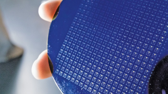
However, the use of diamond power devices has been limited to niche applications due to several challenges. Substrate Growth: The growth of high-quality, large-diameter substrates is crucial for the success of Si power devices. Currently, high-quality diamond substrates are only available in sizes smaller than 1 inch in diameter. The High-Pressure High Temperature (HPHT) process produces expensive substrates (known as Type II) with high purity and low defect density but limited in size to below 1 cm2. Chemical Vapor Deposition (CVD) can be used to create larger diameter wafers, but cost, wafer diameter, and defect density need to be balanced. Diamond substrates commonly used in semiconductor applications are Type 1b wafers, where naturally occurring nitrogen atoms are replaced by isolated carbon atoms. Dislocation densities in diamond can be around 105/cm2, while SiC typically has dislocation densities around 102/cm2.
Doping Challenges: Doping in diamond device fabrication poses a significant bottleneck. Ion implantation only produces shallow doping profiles due to the material characteristics. Doping during CVD growth is preferred but has limitations. The absence of shallow acceptor and donor levels makes it challenging to form highly-doped, activated junctions, particularly for n-type doping. The high activation energy leads to reduced benefits in power density loss compared to SiC, especially at room temperature. The on-state resistance (RDSON) of diamond typically exhibits a negative temperature coefficient (NTC), resulting in NTC total losses. The advantages of diamond in reducing total power conversion losses due to improved dopant activation become significant only at temperatures exceeding 450 K, compared to SiC and GaN. While the NTC of RDSON can have benefits such as lighter heat sinks or transitioning from liquid to air-cooling, it presents challenges in terms of thermal stability and parallelization.
Device and Process Limitations: The high built-in voltage of p-n junctions in diamond (4.9V, compared to 2.8V in SiC) and short carrier lifetimes limit the advantages of bipolar diamond devices to ultra-high voltages (> 6kV) and low switching frequencies. This has shifted the focus to unipolar devices like Schottky diodes. Although significant progress has been made in these devices, they are still limited in terms of breakdown voltages (limited by defects) and exhibit high leakage currents. Novel structures, such as 2DHG (hole gas) based HFETs utilizing the high hole mobility, are under development but face challenges related to doping and device isolation. Diamond power devices also encounter common challenges such as surface passivation and device termination.
Reliability and Packaging: The NTC characteristic necessitates highly thermally coupled paralleled devices. Higher power density losses increase stress on the thermal spreader layer within the package. Moreover, high electric fields can lead to device failures, similar to SiC and GaN devices, requiring further research. The hardness of diamonds also presents challenges for basic failure analysis techniques like TEM sample preparation and die sawing in packaging.
One promising technique that has been developed is the laser slicing of diamond. Assuming high-quality diamond ingots can be produced in the future, an effective wafer-slicing technique will be necessary. In a recent study conducted by Professor Hidai and his team at Chiba University, Japan, a novel laser-based technique for wafer slicing, particularly for {100} surface wafers, has been demonstrated. This technique is crucial for efficient production of high-quality ingots in the future.
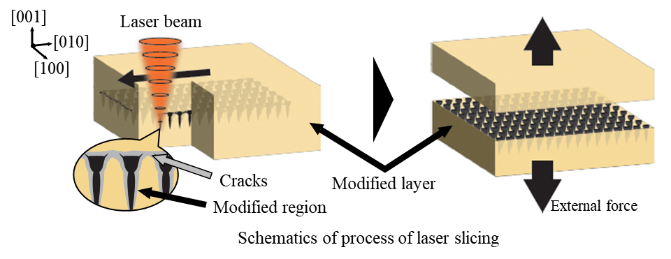
The challenge with slicing wafers in the {100} plane lies in crack propagation along the {111} plane, which leads to increased kerf loss. To address this issue, the researchers employed a 2-step beam approach, which is outlined in Figure 2 of the study. The laser used is Nd:YVO4 with a wavelength of 1064 nm.
In Step 1, an initial 10-pulse beam, with a pulse duration of 11.3 ps and a repetition rate of 10 Hz, is directed 180 um into the surface. This creates modified, amorphous carbon regions in square shapes of approximately 40 um, with a separation of 30 um. Careful consideration is given to choosing the distance between the modified regions to prevent crack formation during this step.
Moving on to Step 2, the laser beam is now adjusted to a pulse width of 46.7 ns and a repetition rate of 30 kHz. It is placed in the space between the square pattern created in Step 1 (refer to Figure 3). This connected the modified regions in an optimal manner, leading to crack formation not only between the modified regions but also ahead of the modified plane, specifically along the {100} cleavage plane. Cracks along the {111} plane are limited in this process.
To create the slice, a sharp needle is subsequently applied to the modified plane. This results in a surface roughness of approximately 20 um. The residual stress in the modified regions depends on the specific irradiation sequence used in steps 1 and 2.
This laser slicing technique can be further refined to improve smoothness and reduce stress. Overall, these advancements hold promise for the future commercialization of diamond semiconductors in power electronics applications.


