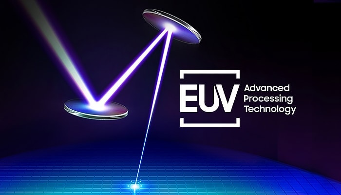
Samsung, a South Korean conglomerate, has recently announced a significant agreement with Dutch semiconductor equipment manufacturer ASML. The deal, valued at KRW 1 trillion (approximately US$755 million), involves the establishment of a semiconductor wafer research factory in South Korea and the development of advanced EUV semiconductor manufacturing technology. This collaboration aims to facilitate the creation of a new generation of EUV semiconductor manufacturing technology.
Kyung Kye-hyun, Vice Chairman and Head of Equipment Solutions Division of Samsung Electronics, highlighted the potential benefits of this agreement, particularly in the acquisition of next-generation High-NA EUV exposure machines. Samsung has reportedly secured priority access to High-NA EUV semiconductor exposure technology, representing a strategic advantage for the company. The partnership is expected to optimize the utilization of High-NA semiconductor exposure technology in the long-term production of DRAM and logic wafers.
The agreement encompasses the construction of a wafer research factory in Gyeonggi-do, South Korea, where engineers from both Samsung and ASML will collaborate to enhance semiconductor production using EUV process technology. Importantly, the focus of the collaboration is not centered on the introduction of 2-nanometer wafer manufacturing equipment to South Korea, but rather on establishing a partnership that enables Samsung to effectively leverage next-generation lithography exposure equipment developed by ASML.
ASML plans to introduce equipment capable of manufacturing 2nm node wafers in the near future. The latest High-NA EUV exposure machine will feature an increased aperture from 0.33 to 0.55, enabling wafer manufacturers to utilize ultra-fine patterning technology in the production of 2-nanometer node wafers. The company aims to produce 10 High-NA EUV machines by 2024, with reports indicating that Intel has already made a significant purchase of 6 of these machines. Additionally, ASML intends to further ramp up the production capacity of this type of semiconductor wafer equipment to 20 sets per year in the coming years.
Following the launch of the ASML High-NA EUV exposure machine, Samsung plans to commence the production of 2nm node process wafers by the end of 2025. It's important to note that, as with any technology and project, the rollout of such chips may be subject to potential delays based on market conditions and the quality of production.


