We will offer a variety of deposition processes and various films with wafer of research and development applications involved in the semiconductor manufacturing process.
Rich processing menu of specialized manufacturer unique will meet the various needs of customers.
In addition, its own super-thick thermal oxide film formation technology is the material that is essential
to the optical device to support the optical communication.
Our products and technologies have been adopted to communication equipment
manufacturers and optical component manufacturers worldwide.
Process Line-up
| Type | Method | Film Type |
|---|---|---|
| Thermal Oxide | Thermal Oxidation | Thin thermal oxide film |
| Super-thick thermal oxide film | ||
| LP-CVD | LP-SiO2 | |
| HTO | ||
| LP-TEOS | ||
| PE-CVD | PE-SiO2 | |
| PE-TEOS | ||
| HDP | ||
| Low-k(BD、BDⅡ、AURORA、CORAL) | ||
| PSG | ||
| NSG | ||
| BPSG | ||
| Spin-coated | SOG | |
| Annealing oven | RTO | |
| Nitride | LP-CVD | LP-SiN |
| PE-CVD | PE-SiN | |
| Si | LP-CVD | Poly-Si |
| Amorphous-Si | ||
| Organic | Spin-coated | G-Line resist |
| I-Line resist | ||
| KrF resist | ||
| ArF resist | ||
| Polyimide(Photosensitive、Non-Photosensitive) | ||
| Metal | Sputter | Al、Al-Si、Al-Si-Cu、Al-Cu |
| Ti、TiN | ||
| Ta、TaN | ||
| Cr | ||
| Cu | ||
| W | ||
| Ni | ||
| Au | ||
| Pt | ||
| ITO | ||
| Plating | Ti、Ni、Au、Cu | |
| CVD | W-Si |
※There are also things that can’t be processed by the wafer size.
※In addition, because the other films can also, please say a hope. Please contact us for details.
| Our Clean Room | |
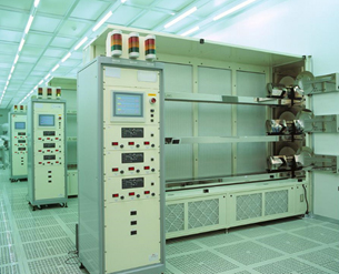 |
 |
 |
|
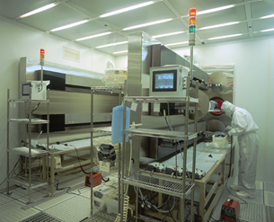
Process Service
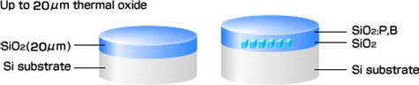
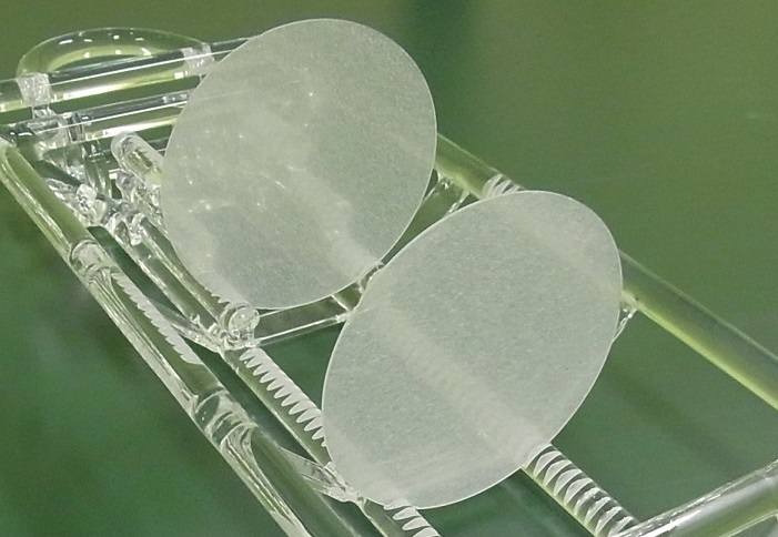
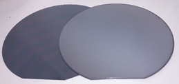
“Super-thick thermal oxide film” applications
Undercladding wafer for AWG
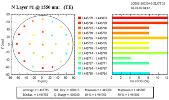
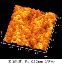
With respect to optical waveguides (AWG), the so-called undercladding layer, which is the lowermost SiO2 film, has a critical effect on the process yield.The Super-thick thermal oxidized films of KST World have the leading share of the global market thanks to their excellent surface cleanliness and stable film quality.
Guaranteed specifications
| Item | Specification |
|---|---|
| Film thickness | 20um±5%(Maximum thickness) |
| In-plane uniformity | ±0.5% |
| Surface uniformity | ±0.5% |
| Refractive index(@1550nm) | 1.4458±0.0001 |
Standard product line-up
| Size | Wafer thickness | Thermal oxidized film thickness |
|---|---|---|
| 4 inches | 525um 1mm | 15um、20um |
| 6 inches | 625um 675um 1mm | 15um、20um |
| 8 inches | 725um | 15um、20um |
| 12 inches | 775um | 15um |
※The above wafer size and thickness, are described our standard products.
※Other sizes and thicknesses are also available. (Up to a maximum thickness of 30μm)
Refractive index plane distribution data
Surface roughness data
Sales of Semiconductor Wafers
We Sales of semiconductor wafers
has a global network for supplying silicon wafers, quartz wafers, compound wafers, and glass substrates to meet the needs of customers. We can also supply tailor-made products. We proposes the most cost-effective products depending on the customer’s application. The silicon wafers, which we use for our own products too, inspected in the clean room. Custmers can rely on the substrate materials we supply.
 |
-Silicon Wafers- For semiconductor and for optical communication, offers as various other product applications. Size and process, you can offer a product that is tailored to your needs, such as the surface orientation and thickness.
|
 |
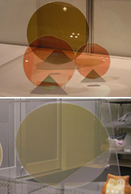
-Glass Substrates-We offer a variety of glass substrates combined with the shape you wish.
|
 |
-Various composite substrate-We, SOQ substrate (Silicon on Quartz), have been made the handling of SOS substrate (Silicon on Sapphire). |
Ion Implantation Services
We can meet widely ranging requirements for ion implantation with various ion implanters and offer analysis services with various analysis devices.
Ion implantation services
| Dopant elements | N、C、F、P、As、B、Ge、Si、Sb、In、O、H、etc |
|---|---|
| Acceleration energy | 200eV ~ 4.6MeV |
※ Constraints of size of wafer may be imposed depending on the measureing equipment.
Analyze services
Sheet resistance measurement, crystal fault detection, surface impurities analysis,
impurities profile analysis, minor constituent analysis, and film thickness measurement
※ Constraints may be imposed depending on the type of ion and size of wafer.
Major facilities
| Devices | Type | Manufacturers |
|---|---|---|
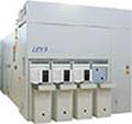
| High current ion implanter | LEX3 | SEN Corporation |
| High current ion implanter | LEX | SEN Corporation |
| High current ion implanter | NV-GDSⅢ-LED | SEN Corporation |
| High current ion implanter | NV-GSD-HC3 | SEN Corporation |
| Medium current ion implanter | MC3シリーズ | SEN Corporation |
| High energy ion implanter | NV-GSD-HE3 | SEN Corporation |
| High energy ion implanter | NV-GSD-HE | SEN Corporation |
| Wafer surface inspection device | LS-6800 | Hitachi High-Technologies Corporation |
| TXRF analyzer | TREX630 | Technos Co., Ltd. |
| ICP-MS | Agilent 7500CS | Yokogawa Analytical Systems, Inc. |
| Wafer review SEM (EDS analysis) | RS-3000 | Hitachi High-Technologies Corporation |
| Scanning electron microscope (EDS analysis) | JSM-5800LV | JEOL Ltd. |
| Sheet resistance measuring equipment | RS-100 | KLA-Tencor Corporation |
| TW measuring equipment | TP630 | KLA-Tencor Corporation |
|
Film thickness measuring device –spectroscopic ellipsometer |
UT-300 | HORIBA, Ltd. |
| RTP | SUMMIT 300XT | Axcelis Technologies |
| RTP | Reliance850 | Axcelis Technologies |
| Vertical furnace | VF-1000 | Koyo Thermo Systems Co., Ltd. |
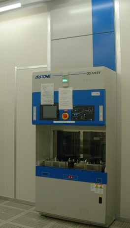
Our Equipment
SOI Wafer of SEIREN KST
SOI(Silicon on Insulator)Wafer is a silicon wafer which is a structured single crystalized layer on oxidized layer and used in the field of high speed LSI, low power LSI, powerdevice, MEMS.
Except for normal SOI, we provide special SOI wafer such as Cavity SOI wafer or Thick BOX SOI wafer.
Cavity SOI will be a good performance on reducing process steps or yield loss, and this would be the possibility for reducing huge cost cutting.
Also, Thick BOX SOI wafer is made by KST’s unique super thick thermal oxidized layer technique which has never been existed before, and possible to make silicon photonics, or super high resistivity powerdevice in the world.
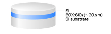
Capability
| Size | 6” 8” |
|---|---|
| Device layer thickness | 100nm※~200μm |
| Wafer in Wafer thickness accuracy | Thin layer ±15nm Thick layer ±0.5μm |
| BOXlayer thickness | Maximum 20μm |
