Welcome to Durham Magneto Optics Ltd. We specialise in advanced scientific instrumentation for nanotechnology research and development. Our product range includes a family of magneto-optical Kerr effect magnetometers (NanoMOKE3) and a family of direct-write optical lithography machines (MicroWriter ML).
Applications of our NanoMOKE3 magnetometers include:
- Magnetic thin films
- Magnetic nanostructures
- Magnetic tunnel junctions
- MRAM
- Hard disk read / write heads
- Spintronic devices
- Magnetic sensors
- Magnetic material development
- Magnetocaloric and thermomagnetic materials
Applications of our MicroWriter ML laser lithography machines include:
- Microelectronics and semiconductor devices
- Spintronics
- MEMS / NEMS
- Sensors
- Microfluidics and lab-on-a-chip
- Materials development
NanoMOKE3 Wafer Mapper
![]()
- Handles up to 200mm wafers (larger sizes available on request)
- Ultra-high sensitivity and stability
- Very low noise
- Highly focused laser spot
- Video-rate microscope to allow precise positioning of laser spot on sample and domain imaging
- 3000 G applied field in x and y or z projected from beneath the wafer allowing free movement of wafer above electromagnet
- Optional heating element to locally inject hot gas at the laser measurement point
- Sensitive to Longitudinal, Transverse and Polar Kerr rotation and ellipticity
- Obtains coercivity, remanence and exchange bias automatically from measured loops
- Supplied with LX Pro, our easy to use and flexible control software
MicroWriter ML3 Baby
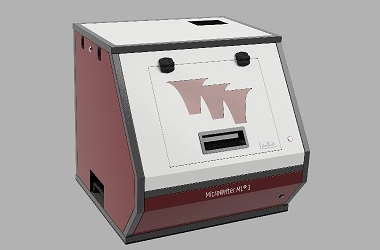
• 149mm x 149mm maximum writing area.
• 155mm x 155mm x 7mm maximum wafer size.
• 1µm minimum feature size across full writing area.
• 405nm long-life semiconductor lightsource suitable for broadband, g- and h-line positive and negative photoresists (e.g. S1800, ECI-3000, MiR 701). Replacement 385nm and 365nm lightsources available as option, suitable for g-, h- and i-line photoresists (e.g. SU-8).
• XY interferometer with 15nm resolution for precise motion control.
• Fast writing speed: up to 50mm2/minute (1µm minimum feature size), allowing a typical 50mm x 50mm area to be exposed in under 1 hour.
• Autofocus system using yellow light with real-time surface tracking laser– no minimum wafer size.
• High quality optical microscope with Olympus infinite conjugate x10 plan objective lens and yellow light illumination for alignment to lithographic markers on the wafer (±2µm 3σ alignment accuracy). Additional x4 digital zoom can be selected in software.
• Grey scale exposure mode for 3-dimensional patterning (255 grey levels).
• Software API for external interfacing and control.
• 200nm minimum addressable grid; 15nm sample stage resolution.
• Acceptable file formats: CIF, GDS2, BMP, TIFF, JPEG, PNG, GIF.
• External dimensions: 700mm (w) x 700mm (d) x 700mm (h), excluding computer.
• Light-excluding enclosure with safety interlock.
• Designed for desktop use – no optical table required.
• Easy to use, Windows® based control software supplied.
• Supplied with KLayout open-source mask design software (www.klayout.de)
• Supplied with pre-configured 64-bit Windows® 10 PC and monitor for ‘plug and play’ installation.
• All cables supplied.
• Extremely competitively priced for University and industrial R&D budgets.
• Can be later upgraded to MicroWriter ML®3 Baby Plus, Mesa or Pro for higher performance.
• CE-marked and compliant with EN-61010.
• 90-260 VAC, 50-60Hz, 4A single phase power requirement.
MicroWriter ML3 Baby Plus

• 149mm x 149mm maximum writing area.
• 155mm x 155mm x 7mm maximum wafer size.
• 1µm and 5µm minimum feature sizes across full writing area.
• Automatic selection of resolution via software – no manual changing of lens required.
• 405nm long-life semiconductor lightsource suitable for broadband, g- and h-line positive and negative photoresists (e.g. S1800, ECI-3000, MiR 701). Replacement 385nm and 365nm lightsources available as option, suitable for g-, h- and i-line photoresists (e.g. SU-8).
• XY interferometer with 15nm resolution for precise motion control.
• Fast writing speed: up to 50mm2/minute (1µm minimum feature size) and 180mm2/minute (5µm minimum feature size), allowing a typical 50mm x 50mm area combining critical and non-critical areas to be exposed in under 30 minutes.
• Autofocus system using yellow light with real-time surface tracking laser– no minimum wafer size.
• High quality infinite conjugate optical microscope camera with x3 aspheric objective lens and x10 Olympus plan objective lens and yellow light illumination for alignment to lithographic markers on the wafer (±1µm 3σ alignment accuracy).
• Automatic changing between microscope magnifications via software – no manual changing of lens required. Additional x4 digital zoom can be selected in software.
• Grey scale exposure mode for 3-dimensional patterning (255 grey levels).
• Software API for external interfacing and control.
• 200nm minimum addressable grid; 15nm sample stage resolution.
• Acceptable file formats: CIF, GDS2, BMP, TIFF, JPEG, PNG, GIF.
• Automatic laser-based wafer centring tool.
• Built-in 2-dimensional optical surface profiler (200nm thickness resolution) for examining exposed resists, deposited layers, etching and other MEMS process steps.
• Automatic wafer inspection tool allowing each die on a wafer to be imaged.
• External dimensions: 700mm (w) x 700mm (d) x 700mm (h), excluding computer.
• Light-excluding enclosure with safety interlock.
• Designed for desktop use – no optical table required.
• Easy to use, Windows® based control software supplied.
• Supplied with KLayout open-source mask design software (www.klayout.de)
• Supplied with pre-configured 64-bit Windows® 10 PC and monitor for ‘plug and play’ installation.
• All cables supplied.
• Extremely competitively priced for University and industrial R&D budgets.
• Can be later upgraded to MicroWriter ML®3 Mesa or Pro for higher performance.
• CE-marked and compliant with EN-61010.
• 90-260 VAC, 50-60Hz, 4A single phase power requirement.
MicroWriter ML3 Mesa

• 149mm x 149mm maximum writing area.
• 155mm x 155mm x 7mm maximum wafer size.
• 0.6µm, 1µm and 5µm minimum feature sizes across full writing area.
• Automatic selection of resolution via software – no manual changing of lens required.
• 405nm long-life semiconductor lightsource suitable for broadband, g- and h-line positive and negative photoresists (e.g. S1800, ECI-3000, MiR 701). Replacement 385nm and 365nm lightsources available as option, suitable for g-, h- and i-line photoresists (e.g. SU-8).
• XY interferometer with 15nm resolution for precise motion control.
• Fast writing speed: up to 17mm2/minute (0.6µm minimum feature size), 50mm2/minute (1µm minimum feature size) and 180mm2/minute (5µm minimum feature size), allowing a typical 50mm x 50mm area combining critical and non-critical areas to be exposed in under 30 minutes.
• Autofocus system using yellow light with real-time surface tracking laser– no minimum wafer size.
• High quality infinite conjugate optical microscope with x3 aspheric objective lens and x10 and x20 Olympus plan objective lens and yellow light illumination for alignment to lithographic markers on the wafer (±1µm 3σ alignment accuracy).
• Automatic changing between microscope magnifications via software – no manual changing of lens required. Additional x4 digital zoom can be selected in software.
• Grey scale exposure mode for 3-dimensional patterning (255 grey levels).
• Software API for external interfacing and control.
• 100nm minimum addressable grid; 15nm sample stage resolution.
• Acceptable file formats: CIF, GDS2, BMP, TIFF, JPEG, PNG, GIF.
• Automatic laser-based wafer centring tool.
• Built-in 2-dimensional optical surface profiler (200nm thickness resolution) for examining exposed resists, deposited layers, etching and other MEMS process steps.
• Automatic wafer inspection tool allowing each die on a wafer to be imaged.
• External dimensions: 700mm (w) x 700mm (d) x 700m (h), excluding computer.
• Light-excluding enclosure with safety interlock.
• Designed for desktop use – no optical table required.
• Easy to use, Windows® based control software supplied.
• Supplied with KLayout open-source mask design software (www.klayout.de)
• Supplied with pre-configured 64-bit Windows® 10 PC and monitor for ‘plug and play’ installation.
• All cables supplied.
• Extremely competitively priced for University and industrial R&D budgets.
• Can be later upgraded to MicroWriter ML®3 Pro for higher performance.
• CE-marked and compliant with EN-61010.
• 90-260 VAC, 50-60Hz, 4A single phase power requirement.
MicroWriter ML3 Pro

• 195mm x 195mm maximum writing area.
• 230mm x 230mm x 15mm maximum wafer size.
• 0.6µm, 1µm, 2µm and 5µm minimum feature sizes across full writing area. 0.4um minimum feature size available as an option.
• Automatic selection of minimum feature size via software – no manual changing of lens required.
• 385nm long-life semiconductor light source, suitable for broadband, g-, h- and i-line positive and negative photoresists (e.g. S1800, ECI-3000, MiR 701, SU-8). Replacement 365nm lightsource available as option for improved performance with SU-8 photoresist.
• XY interferometer with 1nm resolution for precise motion control.
• Extremely fast writing speed – up to: 17mm2/minute (0.6µm minimum feature size), 50mm2/minute (1µm minimum feature size), 120mm2/minute (2µm minimum feature size) and 180mm2/minute (5µm minimum feature size). These allow a typical 50mm x 50mm area combining critical and non-critical areas to be exposed in under 30 minutes or a typical 100mm x 100mm area to be exposed at 2µm minimum feature size in under 2 hours.
• Autofocus system using yellow light with real-time surface tracking laser– no minimum wafer size.
• High quality infinite conjugate optical microscope with x3 aspheric objective lens and x5, x10 and x20 Olympus plan achromatic objective lens and yellow light illumination for alignment to lithographic markers on the wafer (±0.5µm 3σ alignment accuracy). x50 Olympus plan achromatic objective lens available as an option.
• Automatic changing between microscope magnifications via software – no manual changing of lens required. Additional x4 digital zoom can be selected in software.
• Grey scale exposure mode for 3-dimensional patterning (255 grey levels).
• Software API for external interfacing and control.
• 100nm minimum addressable grid; 4nm sample stage resolution.
• Acceptable file formats: CIF, GDS2, BMP, TIFF, JPEG, PNG, GIF.
• Automatic laser-based wafer centring tool.
• Built-in 2-dimensional optical surface profiler (100nm thickness resolution) for examining exposed resists, deposited layers, etching and other MEMS process steps.
• Automatic wafer inspection tool allowing each die on a wafer to be imaged.
• Virtual mask aligner mode in which the pattern to be exposed is displayed on top of the real-time microscope image, allowing the machine to be used like a traditional mask aligner.
• Multiple wafer / chip handling, allowing different exposure patterns and alignment coordinates to be supplied for multiple wafers or chips on the chuck. Used for exposing multiple users’ samples overnight.
• Includes passive vibration-isolation optical table with integrated monitor and keyboard mount.
• Light-excluding enclosure with safety interlock and temperature compensation to ±0.25⁰C
• Easy to use, Windows® based control software supplied.
• Supplied with Clewin 5 mask design software.
• Supplied with pre-configured 64-bit Windows® 10 PC with monitor, keyboard and mouse.
• Includes on-site installation by trained service technician.
• Extremely competitively priced for University and industrial R&D budgets.
• 90-260 VAC, 50-60Hz, 4A single phase power requirement.
• Footprint 90cm (w) x 75cm (d); height 153cm (including optical table)
• CE-marked and compliant with EN-61010.
NanoMOKE3
![]()
- Ultra-high sensitivity and stability
- Very low noise
- Highly focused laser spot
- Video-rate scanning-laser microscope to allow precise positioning of laser spot on sample and high sensitivity domain imaging
- Integrated low noise CCD camera for high quality domain imaging
- Flexible optics and electronics for novel experiments
- 4K-500K cryostat available as an option
- 1200 G applied field in x and y or z; 0.46T field in x available as option
- Sensitive to Longitudinal, Transverse and Polar Kerr rotation and ellipticity
- Supplied with LX Pro, our easy to use and flexible control software
