CMK manufactures Semi-insulating and Semiconducting Gallium Arsenide wafers and ingots by LEC (Liquid Encapsulated Czochralsky) or VGF (Vertical Gradient Freeze) growth method. Required electrical parameters are achieved through high purity 6N input material (Gallium and Arsenic). In order to attain the chosen level of concentration, the dopants like Zinc, Silicon and Tellurium are used.
Ignots
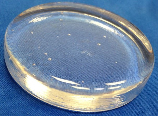
Gallium Arsenide
The production process involves growing of monocrystalline and polycrystalline Gallium Arsenide in PBN and High purity quartz crucibles. We offer monocrystalline wafers and whole ingots with diameter from 2” up to 4“ with quality suitable for epitaxial processing and high-frequency and optoelectronic applications.
High quality material is produced by trained fully qualified staff to meet customer’s often specific needs.
Specification of monocrystalline Gallium Arsenide
GaAs semi-insulating, undoped GaAs semiconducting, p-type & n-type
Diameter wafers: from 2“ up to 4“
ingots & synthesis: from 2“ up to 6“
Thickness wafers: from 325 um up to 750 um
ingots & synthesis: from 2“ up to 6“
Dopant – Zinc, Silicon, Tellurium
Carrier concentration – n-type 1 x 10¹⁶ – 2 x 1018 cm-3
p-type 1 x 10¹⁶ – 5 x 1019 cm-3
Crystal orientation (100), (110), (111)
Off orientation up to 15°, if necessary >15°
Resistivity >1 x 10⁷ Ωcm >1 x 10⁻³ Ωcm
Hall mobility >6000 cm2 V-1s-1 n-type 1 x 10¹⁶ – 2 x 1018 cm-3
p-type 1 x 10¹⁶ – 5 x 1019 cm-3
Etch pit density (EPD) <1 x 104 cm-2 LEC: <7 x 104 cm-2
VGF: <5 x 103 cm-2
Surface treatment wafers: as cut/lapped/etched/single & double side polished ingots and synthesis: as ground/as grown/as cut
Flat orientation US SEMI or EJ standard
Packaging Standard/Empak/Fluoroware/Fluoroware sealed with N2
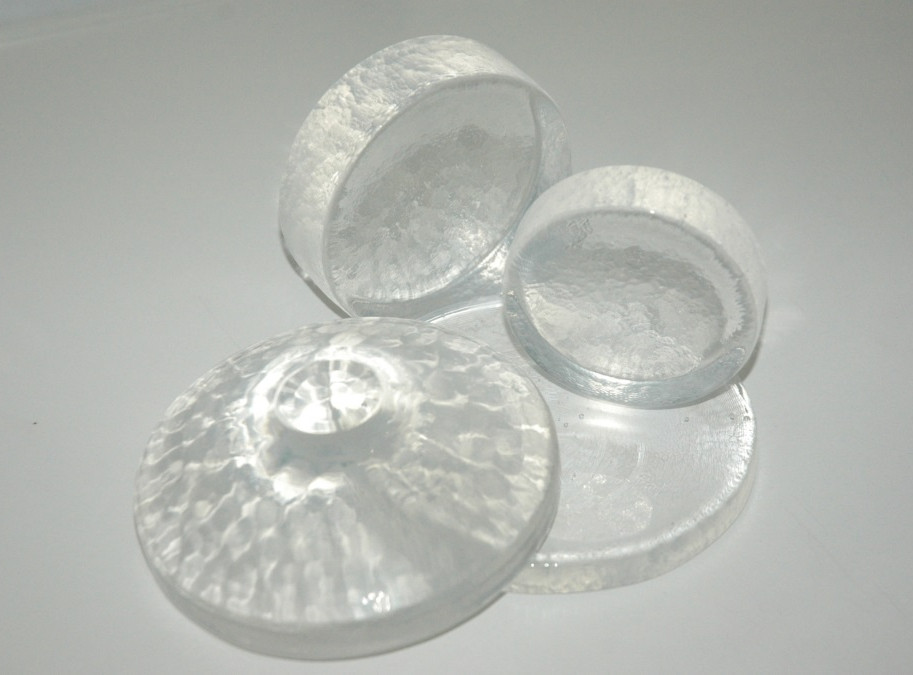
Furthermore, we offer polycrystalline Gallium Arsenide with diameter from 0.5“ up to 4.25“ in the form of wafers and ingots. Our products are manufactured under high pressure with precise stoichiometry control of high purity input material. Each ingot is analyzed using GDMS with the aim to determine the level of its purity.
polycrystalline GaAs ingot
polycrystalline GaAs ingot
Polycrystalline Gallium Arsenide is used as an input material for further processing and applications.
Specification of polycrystalline Gallium Arsenide
GaAs semi-insulating, undoped GaAs semiconducting, p-type & n-type
Diameter wafers: from 0.5“ up to 4.25“
ingots & synthesis: from 2“ up to 6“
Thickness wafers: from 0.5 mm up to 40 mm
ingots & synthesis: from 50mm up to 100mm
Dopant – Zinc, Silicon, Tellurium
Carrier concentration – n-type 1 x 10¹⁶ – 2 x 1018 cm-3
p-type 1 x 10¹⁶ – 5 x 1019 cm-3
Resistivity >1 x 10⁷ Ωcm >1 x 10⁻³ Ωcm
Hall mobility >1 x 103 cm2 V-1s-1 n-type >1500 cm2 V-1 s-1
p-type low
Etch pit density (EPD) <1 x 104 cm-2 LEC: <7 x 104 cm-2
VGF: <5 x 103 cm-2
Surface treatment wafers: as cut/etched ingots and synthesis: as ground/as grown/as cut
Flat orientation US SEMI or EJ standard
Packaging Standard/Fluoroware/Fluoroware sealed with N2
Packaging used for GaAs material
We offer various types of packaging suitable for as cut as well as polished wafers:
Fluoroware individual container,
Fluoroware type tray individually sealed in inert atmosphere,
Empak type 25 wafers box,
Standard type suitable for packaging of whole ingots and crystals;
GaAs packaging
GaAs packaging
Gallium Arsenide field of application
Monocrystalline GaAs
Semi-insulating GaAs
diameter: 2, 3 and 4 inch wafers & ingots
SI undoped
Semiconducting GaAs
diameter: 2, 3 and 4 inch wafers & ingots
SC n-type – Si and Te doped
SC p-type – Zn doped
integrated circuit
LED lightning
Application field: LED industry, High-tech industry, MEMS microelectromechanical systems, Solar products, Active components, Integrated circuits, Telecom parts, etc.
Polycrystalline GaAs
GaAs wafers
diameter: 0.5 – 4.25 inch
thickness: 0.5 mm – 40 mm
SI undoped
SC n-type Si and Te doped, p-type Zn doped
GaAs Ingots up to 6“ for VGF growing
diameter: 4.5 – 6 inch
thickness: 50 – 100 mm
SI undoped
SC n-type Si and Te doped, p-type Zn doped
Growth method: LEC and VGF
solar cells
solar cells
Application field: Polycrystalline GaAs is used as a starting material for the manufacture of GaAs products (LED industry, Fiber optic communication, Microwave circuits, Solar cells application, High efficiency photovoltaic devices, etc.)
Blanks for Optical Components
Opto GaAs wafers
diameter: 0.5 – 4.25 inch
thickness: 1 mm – 20 mm
SI undoped
Growth method: LEC
Application field: Wireless communication, PHEMT technology, Opto-electronic components (Photodiodes, Phototransistors, Photoresistors, Integrated optical circuits, Optocoupler, Laser diodes, Infrared emitting diodes), Chips, Optical fiber communication, Solar products, etc.
CMK usually offers metallic Gallium in high quality, which is required in semiconductor industry. The flexibility of our refining technology allows also the modification of the product purity according to the customer’s requirement, therefore the Gallium in 5N, 6N, 6N+ or 7N purity can be produced.
CMK offers the service of refining, where the supplied low purity Gallium from the customer is refined to high purity Gallium. Related to Gallium also a service of recycling is used, where the Gallium is recaptured from the waste containing this metal.
After gaining Gallium in required quality, it is packed in a box under pure nitrogen atmosphere and shipped in HDPE bottles of various size and weight.
Diboron Trioxide (B2O3) s produced from high purity boric acid. It is used for GaAs production. But there is also a demand from the customers, who deal with the GaP and/or InAs crystal growing processes using both LEC and/or VGF methods.
The purity of our product was determined using GDMS and it was evaluated as 99.995 – 99.999 %.
Specification of our standard produced pellets.
| Product moisture (ppm weight) |
| Range of water content | I. 100 – 300 |
II. 301 – 500 |
III. 501 – 1000 |
IV. > 1000 |
| Deviation is determined to be: +/- 10 %. |
| Dimension and weight of cylinder and tapered pellets |
| Diameter, mm | 50 | 83 | 100 | 138 |
| Weight, g | 55 | 100 – 200 | 400 | 400 – 700 |
| Deviation for diameter is determined to be: +/- 2 mm, deviation for weight is determined to be: +/- 3 %. |
The services we are offering are closely bound to our activities. Our skilful staff is involved mainly in the service of recycling of many GaAs material/waste types, refining of the Gallium metal up to 99.99999 % and our analytical services.
