Kulicke & Soffa (NASDAQ: KLIC) is a leading provider of semiconductor and electronic assembly solutions serving the global automotive, consumer, communications, computing and industrial markets. Founded in 1951, K&S prides itself on establishing foundations for technological advancement - creating pioneering interconnect solutions that enable performance improvements, power efficiency, form-factor reductions and assembly excellence of current and next-generation semiconductor devices.
Leveraging decades of development proficiency and extensive process technology expertise, Kulicke & Soffa’s expanding portfolio provides equipment solutions, aftermarket products and services supporting a comprehensive set of interconnect technologies including wire bonding, advanced packaging, lithography, and electronics assembly. Dedicated to empowering technological discovery, always, K&S collaborates with customers and technology partners to push the boundaries of possibility, enabling a smarter future.
ADVANCED PACKAGING WITH ADAPTIVE MACHINE ANALYTICS - MORE THAN BONDING
As features and functionalities of ICs increases, driving higher I/Os, the trend for flip chip is moving towards pitches less than 100 μm needing higher accuracy flip chip bonding and alternative interconnect solutions. Designed with performance and accuracy in mind, K&S APAMA™ Plus Thermo-Compression Bonding (TCB) solutions provide higher accuracy and lower pitch bonding with market leading throughput.
The APAMA Series offers fully Automated Chip-to-Substrate (C2S) and Chip-to-Wafer (C2W) solutions for Thermo-Compression Bonding (TCB).
HIGHEST ACCURACY, HIGHEST UPH FLIP-CHIP PERFORMANCE
Kulicke & Soffa's Katalyst™ delivers the industry's highest accuracy and speed for flip-chip placement. Its hardware and technology enable < 3 μm accuracy on substrate or wafer, achieving the best Cost-of-Ownership in the industry.
Key Features:
- Best-in-industry flip-chip at 15K UPH Sprint with 3 μm accuracy
- Ease-of-use Automated Recipe with fully guided Setup Wizards
- Automated , UPH neutral Accuracy Calibration, to avoid nozzle-to-nozzle variations during runtime
- Automated thermal Drift Compensation
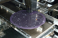
Wafer Level Packaging (WLP)
- Bonding Flip Chips and/or Passives onto wafers or panels
- Processing wafers sizes up to 12" and larger
- Cam-X and Secs-Gem compatible
- Feeding from wafer, waffle pack, tray or tape and reel
- Full controlled Placement force for thin Flip Chips or low profile passives
- Full traceability
- Fine pitch Copper Pillar Bumps
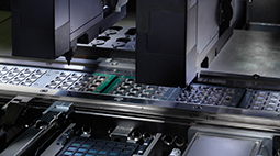
MCM & SIP/FC BGA/FC-CSP/ FC-Memory/FCOB
- Up to 27,000 cph (IPC) Flip Chip bonding speeds
- Up to 140,000 cph (IPC) Chip shooting speeds
- High quality pick and placement process
- 7 Micron for Flips Chips, Die and Wafer Level Packages
- Full controlled Placement force for thin Flip Chips or low profile passives
- Feeding from wafer, waffle pack, tray or tape and reel
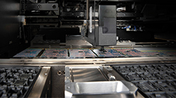
POP (Package-on-Package)
- Die or BGA stacking at the highest throughput on smallest footprint
- Feeding from wafer, waffle pack, tray or tape and reel
- Full force control with every Placement at all placement height
- Easy to exchange linear flux unit
Kulicke & Soffa's ball bonders are the leading generation of semiconductor assembly equipment for today's most challenging applications. With our long-standing tradition of innovation and technology leadership, the K&S ball bonders set new standards for performance, productivity, reliability, and ease of use.
K&S Lithography brings you a breakthrough in Lithography for Advanced Packaging by developing a dedicated solution with a major reduction in Cost-of-Ownership.
Key Features & Benefits of the LITEQ 500 projection stepper
- Highest Throughput
- Up to 2x better Cost of Ownership
- Laser based light source
- Innovative optical design
- High speed wafer handling
- Modular system architecture
- Differentiating software
